|
|
|
PDF ADS1202IPWR Data sheet ( Hoja de datos )
| Número de pieza | ADS1202IPWR | |
| Descripción | Motor Control Current Shunt 1-Bit/ 10MHz/ 2nd-Order/ Delta-Sigma Modulator | |
| Fabricantes | Burr-Brown Corporation | |
| Logotipo | ||
Hay una vista previa y un enlace de descarga de ADS1202IPWR (archivo pdf) en la parte inferior de esta página. Total 21 Páginas | ||
|
No Preview Available !
ADS1202
SBAS275 – DECEMBER 2002
Motor Control Current Shunt
1-Bit, 10MHz, 2nd-Order, Delta-Sigma Modulator
FEATURES
q 16-BIT RESOLUTION
q 13-BIT LINEARITY
q RESOLUTION/SPEED TRADE-OFF:
10-Bit Effective Resolution with 20µs Signal
Delay (12-bit with 77µs)
q ±250mV INPUT RANGE WITH SINGLE 5V SUPPLY
q 2% INTERNAL REFERENCE VOLTAGE
q 2% GAIN ERROR
q FLEXIBLE SERIAL INTERFACE WITH FOUR
DIFFERENT MODES
q IMPLEMENTED TWINNED BINARY CODING AS
SPLIT PHASE OR MANCHESTER CODING FOR
ONE LINE INTERFACING
q OPERATING TEMPERATURE RANGE:
–40°C to +85°C
DESCRIPTION
The ADS1202 is a precision, 80dB dynamic range, delta-
sigma (∆∑) modulator operating from a single +5V supply.
The differential inputs are ideal for direct connections to
transducers or low-level signals. With the appropriate digital
filter and modulator rate, the device can be used to achieve
16-bit Analog-to-Digital (A/D) conversion with no missing
codes. Effective resolution of 12 bits can be maintained with
a digital filter bandwidth of 10kHz at a modulator rate of
10MHz. The ADS1202 is designed for use in medium reso-
lution measurement applications including current measure-
ments, smart transmitters, industrial process control, weigh
scales, chromatography, and portable instrumentation. It is
available in a TSSOP-8 package.
APPLICATIONS
q MOTOR CONTROL
q CURRENT MEASUREMENT
q INDUSTRIAL PROCESS CONTROL
q INSTRUMENTATION
q SMART TRANSMITTERS
q PORTABLE INSTRUMENTS
q WEIGHT SCALES
q PRESSURE TRANSDUCERS
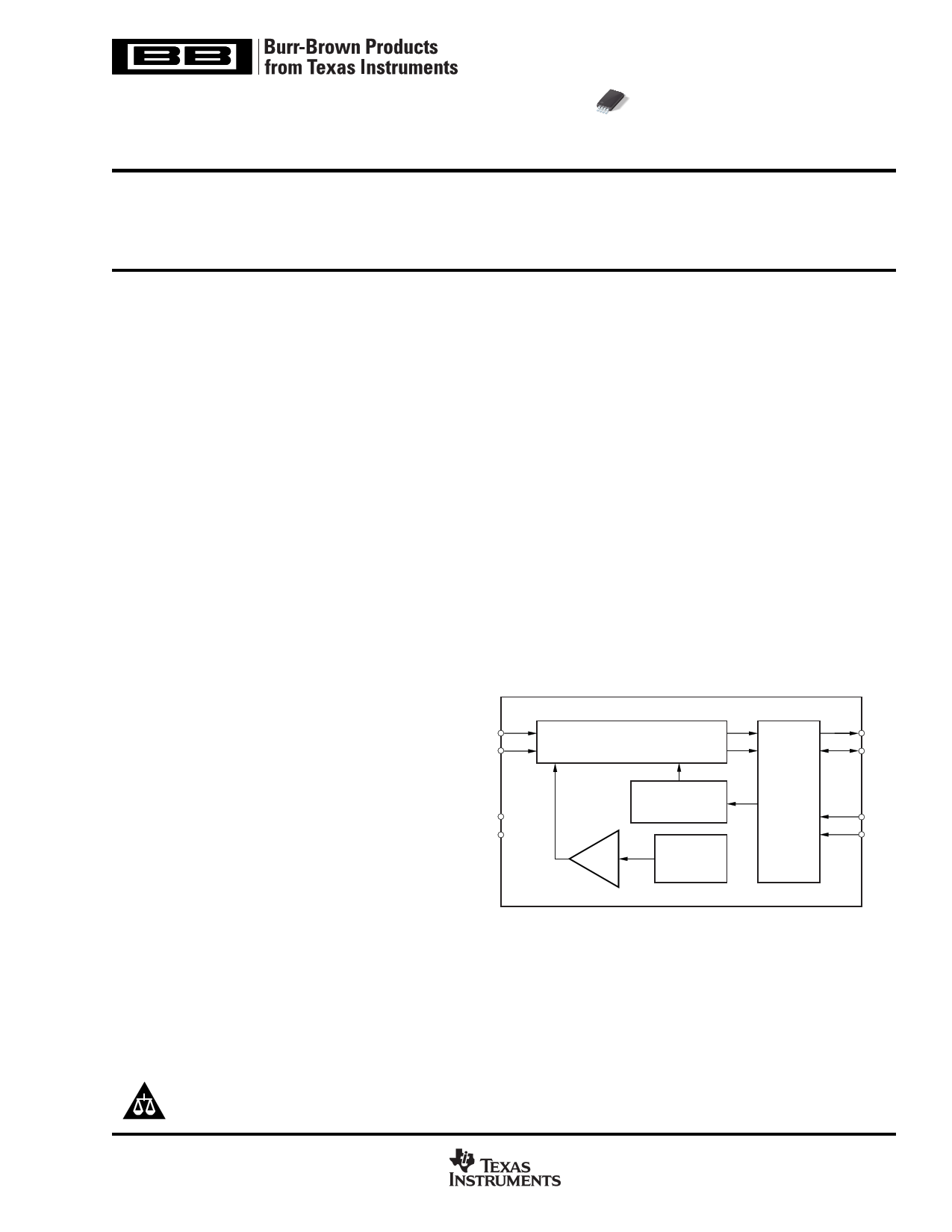
VIN+
VIN–
VDD
GND
2nd-Order
∆∑ Modulator
Buffer
RC Oscillator
20MHz
Reference
Voltage
2.5V
Interface
Circuit
MDAT
MCLK
M0
M1
Please be aware that an important notice concerning availability, standard warranty, and use in critical applications of
Texas Instruments semiconductor products and disclaimers thereto appears at the end of this data sheet.
PRODUCTION DATA information is current as of publication date.
Products conform to specifications per the terms of Texas Instruments
standard warranty. Production processing does not necessarily include
testing of all parameters.
www.ti.com
Copyright © 2002, Texas Instruments Incorporated
1 page 
TIMING DIAGRAMS (Cont.)
MCLK
MDAT
tC4
tw4
tD4
DIAGRAM 4: Mode 3 Operation.
TIMING CHARACTERISTICS
over recommended operating free-air temperature range –40°C to +85°C, VDD = 5V, and MCLK = 10MHz, unless otherwise noted.
SPEC
DESCRIPTION
MODE
MIN
MAX
UNITS
tC1 Clock Period
tW1 Clock HIGH Time
tD1 Data delay after rising edge of clock
tC2 Clock Period
tW2 Clock HIGH Time
tD2 Data delay after rising edge of clock
tD3 Data delay after falling edge of clock
tC3 Clock Period
tW3 Clock HIGH Time
tC4 Clock Period
tW4 Clock HIGH Time
tD4 Data delay after falling edge of clock
tR1 Rise Time of Clock
tF1 Fall Time of Clock
0 90
110
0 tC1/2 – 5 tC1/2 + 5
0
tC1/4 – 10
tC1/4 + 10
1 180
220
1 tC2/2 – 5 tC2/2 + 5
1
tC2/4 – 10
tC2/4 + 10
1
tC2/4 – 10
tC2/4 + 10
2 90
110
2 tC3/2 – 5 tC3/2 + 5
3 45
55
3 10 tC4 – 10
30
10
30
10
30
10
ns
ns
ns
ns
ns
ns
ns
ns
ns
ns
ns
ns
ns
ns
NOTE: All input signals are specified with tR = tF = 5ns (10% to 90% of VDD) and timed from a voltage level of (VIL + VIH)/2. See timing diagrams 1 thru 4.
ADS1202
SBAS275
www.ti.com
5
5 Page 
ANALOG INPUT STAGE
Analog Input
The input design topology of the ADS1202 is based on a fully
differential switched-capacitor architecture. This input stage
provides the mechanism to achieve low system noise, high
common-mode rejection (90dB), and excellent power-supply
rejection. The input impedance of the analog input is depen-
dant on the input capacitor and modulator clock frequency
(MCLK), which is also the sampling frequency of the modu-
lator. Figure 2 shows the basic input structure of the ADS1202.
The relationship between the input impedance of the ADS1202
and the modulator clock frequency is:
AIN(Ω)
=
7
•
1012
fMCLK (MHz)
(1)
The input impedance becomes a consideration in designs
where the source impedance of the input signal is HIGH. In
this case, it is possible for a portion of the signal to be lost
across this external source impedance. The importance of this
effect depends on the desired system performance. There are
two restrictions on the analog input signal to the ADS1202.
Under no conditions should the current into or out of the
analog inputs exceed 10mA. The absolute input voltage range
must stay in the range GND – 0.4V to VDD + 0.3V. If either of
the inputs exceed these limits, the input protection diodes on
the front end of the converter will begin to turn on. In addition,
the linearity of the device is ensured only when the analog
voltage applied to either input resides within the range defined
by –320mV and +320mV.
Modulator
The modulator sampling frequency (CLK) can be operated
over a range of a few MHz to 12MHz in mode 3. The
frequency of MCLK can be decreased to adjust for the clock
requirements of the application. The external MCLK must
have double the modulator frequency.
The modulator topology is fundamentally a 2nd-order, charge-
balancing A/D converter, as the one conceptualized in Figure 3.
The analog input voltage and the output of the 1-bit Digital-to-
Analog Converter (DAC) are differentiated, providing an analog
voltage at X2 and X3. The voltage at X2 and X3 are presented
to their individual integrators. The output of these integrators
progress in a negative or positive direction. When the value of
the signal at X4 equals the comparator reference voltage, the
output of the comparator switches from negative to positive, or
positive to negative, depending on its original state. When the
output value of the comparator switches from HIGH to LOW or
vice versa, the 1-bit DAC responds on the next clock pulse by
changing its analog output voltage at X6, causing the integrators
to progress in the opposite direction. The feedback of the
modulator to the front end of the integrators forces the value of
the integrator output to track the average of the input.
AIN+
Switching Frequency
= CLK
AIN–
RSW
350kΩ (typ)
1.5pF
CINT
7pF (typ)
High
Impedance
> 1GΩ
VCM
1.5pF
RSW
350kΩ (typ)
CINT
7pF (typ)
High
Impedance
> 1GΩ
FIGURE 2. Input Impedance of the ADS1202.
X(t) X2
Integrator 1
fS
X3
Integrator 2
X4
VREF
fCLK
DATA
Comparator
X6 D/A Converter
FIGURE 3. Block Diagram of the 2nd-Order Modulator.
ADS1202
SBAS275
www.ti.com
11
11 Page | ||
| Páginas | Total 21 Páginas | |
| PDF Descargar | [ Datasheet ADS1202IPWR.PDF ] | |
Hoja de datos destacado
| Número de pieza | Descripción | Fabricantes |
| ADS1202IPWR | Motor Control Current Shunt 1-Bit/ 10MHz/ 2nd-Order/ Delta-Sigma Modulator | Burr-Brown Corporation |
| ADS1202IPWT | Motor Control Current Shunt 1-Bit/ 10MHz/ 2nd-Order/ Delta-Sigma Modulator | Burr-Brown Corporation |
| Número de pieza | Descripción | Fabricantes |
| SLA6805M | High Voltage 3 phase Motor Driver IC. |
Sanken |
| SDC1742 | 12- and 14-Bit Hybrid Synchro / Resolver-to-Digital Converters. |
Analog Devices |
|
DataSheet.es es una pagina web que funciona como un repositorio de manuales o hoja de datos de muchos de los productos más populares, |
| DataSheet.es | 2020 | Privacy Policy | Contacto | Buscar |