|
|
|
PDF ADVFC32 Data sheet ( Hoja de datos )
| Número de pieza | ADVFC32 | |
| Descripción | Voltage-to-Frequency and Frequency-to-Voltage Converter | |
| Fabricantes | Analog Devices | |
| Logotipo | ||
Hay una vista previa y un enlace de descarga de ADVFC32 (archivo pdf) en la parte inferior de esta página. Total 7 Páginas | ||
|
No Preview Available !
a
FEATURES
High Linearity
؎0.01% Max at 10 kHz FS
؎0.05% Max at 100 kHz FS
؎0.2% Max at 500 kHz FS
Output TTL/CMOS-Compatible
V/F or F/V Conversion
6 Decade Dynamic Range
Voltage or Current Input
Reliable Monolithic Construction
MIL-STD-883-Compliant Versions Available
Voltage-to-Frequency and
Frequency-to-Voltage Converter
ADVFC32
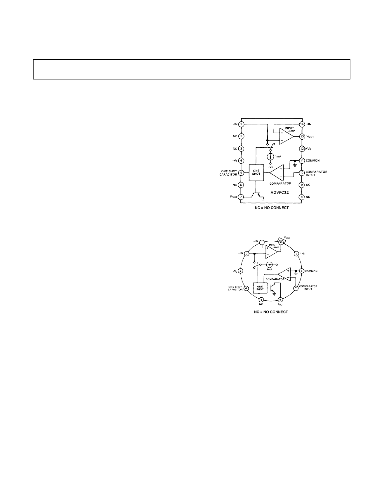
PIN CONFIGURATION
(TOP VIEW)
N-14 Package
PRODUCT DESCRIPTION
The industry standard ADVFC32 is a low cost monolithic
voltage-to-frequency (V/F) converter or frequency-to-voltage
(F/V) converter with good linearity (0.01% max error at 10 kHz)
and operating frequency up to 0.5 MHz. In the V/F configuration,
positive or negative input voltages or currents can be converted
to a proportional frequency using only a few external compo-
nents. For F/V conversion, the same components are used with
a simple biasing network to accommodate a wide range of input
logic levels.
TTL or CMOS compatibility is achieved in the V/F operating
mode using an open collector frequency output. The pull-up
resistor can be connected to voltages up to 30 volts, or to 15 V
or 5 V for conventional CMOS or TTL logic levels. This resis-
tor should be chosen to limit current through the open collector
output to 8 mA. A larger resistance can be used if driving a high
impedance load.
Input offset drift is only 3 ppm of full scale per °C, and full-
scale calibration drift is held to a maximum of 100 ppm/°C
(ADVFC32BH) due to a low T.C. Zener diode.
The ADVFC32 is available in commercial, industrial, and
extended temperature grades. The commercial grade is pack-
aged in a 14-lead plastic DIP while the two wider temperature
range parts are packaged in hermetically sealed 10-lead cans.
PRODUCT HIGHLIGHTS
1. The ADVFC32 uses a charge balancing circuit technique
(see Functional Block Diagram) which is well suited to high
accuracy voltage-to-frequency conversion. The full-scale
operating frequency is determined by only one precision
resistor and capacitor. The tolerance of other support compo-
nents (including the integration capacitor) is not critical.
Inexpensive ± 20% resistors and capacitors can be used with-
out affecting linearity or temperature drift.
H-10A Package
2. The ADVFC32 is easily configured to satisfy a wide range of
system requirements. Input voltage scaling is set by selecting
the input resistor which sets the input current to 0.25 mA at
the maximum input voltage.
3. The same components used for V/F conversion can also be
used for F/V conversion by adding a simple logic biasing
network and reconfiguring the ADVFC32.
4. The ADVFC32 is intended as a pin-for-pin replacement for
VFC32 devices from other manufacturers.
5. The ADVFC32 is available in versions compliant with MIL-
STD-883. Refer to the Analog Devices Military Products
Databook or current ADVFC32/883B data sheet for detailed
specifications.
REV. B
Information furnished by Analog Devices is believed to be accurate and
reliable. However, no responsibility is assumed by Analog Devices for its
use, nor for any infringements of patents or other rights of third parties
which may result from its use. No license is granted by implication or
otherwise under any patent or patent rights of Analog Devices.
One Technology Way, P.O. Box 9106, Norwood, MA 02062-9106, U.S.A.
Tel: 781/329-4700 World Wide Web Site: http://www.analog.com
Fax: 781/326-8703
© Analog Devices, Inc., 2000
1 page 
ADVFC32
Input resistance RIN is composed of a fixed resistor (R1) and a
variable resistor (R3) to allow for initial gain error compensation.
To cover all possible situations, R3 should be 20% of RIN, and
R1 should be 90% of RIN. This allows a ± 10% gain adjustment
to compensate for the ADVFC32 full-scale error and the toler-
ance of C1.
If more accurate initial offset is required, the circuit of R4 and
R5 can be added. R5 can have a value between 10 kΩ and
100 kΩ, and R4 should be approximately 10 MΩ. The amount
of current required to trim zero offset will be relatively small, so
the temperature coefficients of these resistors are not critical. If
large offsets are added using this circuit, temperature drift of
both of these resistors is much more important.
BIPOLAR V/F
By adding another resistor from Pin 1 (Pin 2 of TO-100 can) to
a stable positive voltage, the ADVFC32 can be operated with a
bipolar input voltage. For example, an 80 kΩ resistor to 10 V
causes an additional current of 0.125 mA to flow into the inte-
grator so that the net current flow to the integrator is positive
even for negative input voltages. At negative full-scale input
voltage, 0.125 mA will flow into the integrator from VIN cancel-
ling out the 0.125 mA from the offset resistor, resulting in an
output frequency of zero. At positive full scale, the sum of the
two currents will be 0.25 mA and the output will be at its maxi-
mum frequency.
F/V CONVERSION
Although the mathematics of F/V conversion can be very com-
plex, the basic principle is easy to understand. Figure 4 shows
the connection diagram for F/V conversion with TTL input
logic levels. Each time the input signal crosses the comparator
threshold going negative, the one shot is activated and switches
1 mA into the integrator input for a measured time period
(determined by C1). As the frequency increases, the amount of
charge injected into the integration capacitor increases propor-
tionately. The voltage across the integration capacitor is stabilized
when the leakage current through R1 and R3 equals the average
current being switched into the integrator. The net result of
these two effects is an average output voltage which is propor-
tional to the input frequency. Optimum performance can be
obtained by selecting components using the same guidelines and
equations listed in the V/F conversion section.
UNIPOLAR V/F, NEGATIVE INPUT VOLTAGE
Figure 3 shows the connection diagram for V/F conversion of
negative input voltages. In this configuration full-scale output
frequency occurs at negative full-scale input, and zero output
frequency corresponds to zero input voltage.
Figure 4. Connection Diagram for F/V Conversion, TTL
Input
Figure 3. Connection Diagram for V/F Conversion,
Negative Input Voltage
A very high impedance signal source may be used since it only
drive the noninverting integrator input. Typical input imped-
ance at this terminal is 250 MΩ or higher. For V/F conversion
of positive input signals the signal generator must be able to
source 0.25 mA to properly drive the ADVFC32, but for nega-
tive V/F conversion the 0.25 mA integration current is drawn
from ground through R1 and R3.
Circuit operation for negative input voltages is very similar to
positive input unipolar conversion described in the previous
section. For best operating results use component equations
listed in that section.
DECOUPLING
Decoupling power supplies at the device is good practice in any
system, but absolutely imperative in high resolution applica-
tions. For the ADVFC32, it is important to remember where
the voltage transients and ground currents flow. For example,
the current drawn through the output pull-down transistor
originates from the logic supply, and is directed to ground
through Pin 11 (Pin 8 of TO-100). Therefore, the logic supply
should be decoupled near the ADVFC32 to provide a low im-
pedance return path for switching transients. Also, if there is a
separate digital ground it should be connected to the analog
ground at the ADVFC32. This will prevent ground offsets that
could be created by directing the full 8 mA output current into
the analog ground, and subsequently back to the logic supply.
Although some circuits may operate satisfactorily with the power
supplies decoupled at only one location on each board, this
practice is not recommended for the ADVFC32. For best results,
each supply should be decoupled with 0.1 µF capacitor at the
ADVFC32. In addition, a larger board level decoupling capaci-
tor of 1 µF to 10 µF should be located relatively close to the
ADVFC32 on each power supply.
COMPONENT TEMPERATURE COEFFICIENTS
The drift specifications of the ADVFC32 do not include tem-
perature effects of any of the supporting resistors or capacitors.
The drift of the input resistors R1 and R3 and the timing capaci-
tor C1 directly affect the overall temperature stability. In the
–4– REV. B
5 Page | ||
| Páginas | Total 7 Páginas | |
| PDF Descargar | [ Datasheet ADVFC32.PDF ] | |
Hoja de datos destacado
| Número de pieza | Descripción | Fabricantes |
| ADVFC32 | Voltage-to-Frequency and Frequency-to-Voltage Converter | Analog Devices |
| Número de pieza | Descripción | Fabricantes |
| SLA6805M | High Voltage 3 phase Motor Driver IC. |
Sanken |
| SDC1742 | 12- and 14-Bit Hybrid Synchro / Resolver-to-Digital Converters. |
Analog Devices |
|
DataSheet.es es una pagina web que funciona como un repositorio de manuales o hoja de datos de muchos de los productos más populares, |
| DataSheet.es | 2020 | Privacy Policy | Contacto | Buscar |