|
|
|
PDF NAU82028 Data sheet ( Hoja de datos )
| Número de pieza | NAU82028 | |
| Descripción | 3.1W Mono Filter-Free Class-D Audio Amplifier | |
| Fabricantes | nuvoton | |
| Logotipo | ||
Hay una vista previa y un enlace de descarga de NAU82028 (archivo pdf) en la parte inferior de esta página. Total 19 Páginas | ||
|
No Preview Available !
NAU82028
3.1W Mono Filter-Free Class-D Audio Amplifier
with 2 wire interface gain control
1 Description
The NAU82028 is a mono high efficiency filter-free Class-D audio amplifier, which is capable of driving a 4Ω load with
up to 3.1W output power. This device provides chip enable pin with extremely low standby current and fast start-up time
of 3.4ms. The NAU82028 features a highly flexible 2 wire interface with many useful gain settings. The gain can be
selected from 12dB to –20.5dB (plus mute) by using 2 wire interface.
The NAU82028 is ideal for the portable applications of battery drive, as it has advanced features like 93% efficiency,
ultra low quiescent current (i.e. 2.0 mA at 3.6V) and superior EMI performance. It has the ability to configure the inputs
in either single-ended or differential mode.
NAU82028 is available in Miniature WCSP-9 (1.56mm x 1.52mm in 0.5mm pitch) package.
Key Features
Low Quiescent Current:
2.0mA at 3.6V
3.1mA at 5V
Gain Setting with 2 wire interface
12dB to -19.3dB (plus mute)
Powerful Mono Class-D Amplifier:
3.1W (4Ω @ 5V, 10% THD+N)
2.46W (4Ω @ 5V, 1% THD+N)
1.77W (8Ω @ 5V, 10% THD+N)
1.41W (8Ω @ 5V, 1% THD+N)
1.54 W (4Ω @ 3.6V, 10% THD+N)
1.26 W (4Ω @ 3.6V, 1% THD+N)
0.9 W (8Ω @ 3.6V, 10% THD+N)
0.76 W (8Ω @ 3.6V, 1% THD+N)
Low Output Noise: 26 µVRMS (A –Weighted @3.6V)
Low Current Shutdown Mode
Click-and Pop Suppression
1.56mm x 1.52mm in WCSP (0.5mm Pitch)
Applications
Smartphones
Tablet PCs
Personal Navigation Devices
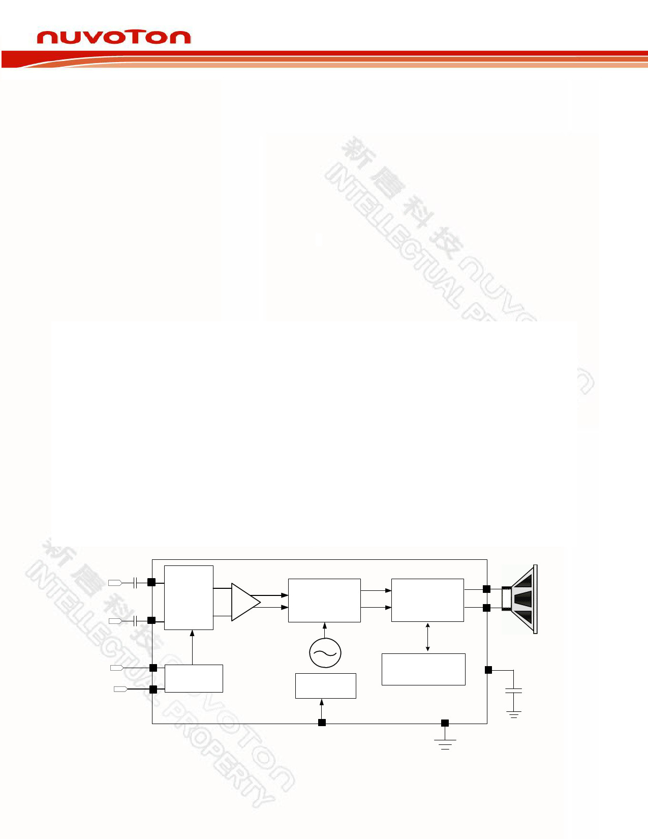
VIN
VIP
Gain
Control
Class D
Modulator
Output
Driver
SCL
SDA
2 Wire
Control
NAU82028
Click / Pop
Suppression
EN
NAU82028 Datasheet Rev 0.2
Page 1 of 19
Current / Thermal
Protection
VSS
VDD
Mar, 2013
1 page 
Two wire control mode timing
Symbol
TSTAH
TSTAS
TSTOS
TSCLH
TSCLL
TRISE
TFALL
TSDAS
TSDAH
Description
SDA falling edge to SCL falling edge hold timing in
START / Repeat START condition
SCL rising edge to SDA falling edge setup timing in
Repeat START condition
SCL rising edge to SDA rising edge setup timing in
STOP condition
SCL High Pulse Width
SCL Low Pulse Width
Rise Time for all 2-wire Mode Signals
Fall Time for all 2-wire Mode Signals
SDA to SCL Rising Edge DATA Setup Time
SCL falling Edge to SDA DATA Hold Time
Digital Serial Interface Electrical Characteristics
Condition
Min Typ.
Max. Unit
Input Leakage Current
SCL, SDA
-1
-
+1 A
Input High Voltage VIH
0.7
VDD
5.5 V
Input low Voltage VIL VSS
0.3 VDD V
VOH (SCL, SDA)
0.9
VDD
V
VOL (SCL, SDA)
0.2 VDD V
SDA, SCL; pull up
resistor value
50k
Ohm
The following setup is used to measure the above parameters
VDD
Min Typ Max Unit
600 - - ns
600 - - ns
600 - - ns
600
1,300
-
-
100
0
-
-
-
-
-
-
- ns
- ns
300 ns
300 ns
- ns
600 ns
Test Conditions
VDD = 5.5V
IOL = 1 mA
+
Audio Precision
Output
-
1uF
1uF
NAU82028
30kHz RC
ZL Low pass filter
+
Audio Precision
Input
-
NAU82028 Datasheet Rev0.2
Page 5 of 19
Mar, 2013
5 Page 
5.1.1 2-Wire-Serial Control and Data Bus (I2C Style Interface)
The serial interface provides a 2-wire bidirectional read/write data interface similar to and typically compatible with
standard I2C protocol. This protocol defines any device that sends CLK onto the bus as a master, and the receiving
device as slave. The NAU82028 can function only as a slave device.
An external clock drives the device, and in accordance with the protocol, data is sent to or from the device accordingly.
All functions are controlled by means of a register control interface in the device.
5.1.2 2-Wire Protocol Convention
All 2-Wire interface operations must begin with a START condition, which is a HIGH-to-LOW transition of SDA while
SCL is HIGH. All 2-Wire interface operations are terminated by a STOP condition, which is a LOW to HIGH transition
of SDA while SCL is HIGH. A STOP condition at the end of a read or write operation places the serial interface in
standby mode.
An acknowledge (ACK), is a software convention is used to indicate a successful data transfer. The transmitting device
releases the SDA bus after transmitting eight bits to allow for the ACK response. During the ninth clock cycle, the
receiver pulls the SDA line LOW to acknowledge the reception of the eight bits of data.
Following a START condition, the master must output a device address byte. This consists of a 7-bit device address, and
the LSB of the device address byte is the R/W (Read/Write) control bit. When R/W= 1, this indicates the master is
initiating a read operation from the slave device, and when R/W=0, the master is initiating a write operation to the slave
device. If the device address matches the address of the slave device, the slave will output an ACK during the period
when the master allows for the ACK signal.
SDA
SCL
START
START and STOP signals
STOP
Not Acknowledge
SDA
Acknowledge
SCL
18
2 ...7
9
Acknowledge and NOT Acknowledge
010101
A7 A6 A5 A4 A3 A2
D7 D6 D5 D4 D3 D2
0
R/W
Device
Address Byte
A1
A0
Control
Address Byte
D1 D0 Data Byte
Slave Address Byte, Control Address Byte, and Data Byte
NAU82028 Datasheet Rev0.2
Page 11 of 19
Mar, 2013
11 Page | ||
| Páginas | Total 19 Páginas | |
| PDF Descargar | [ Datasheet NAU82028.PDF ] | |
Hoja de datos destacado
| Número de pieza | Descripción | Fabricantes |
| NAU82028 | 3.1W Mono Filter-Free Class-D Audio Amplifier | nuvoton |
| Número de pieza | Descripción | Fabricantes |
| SLA6805M | High Voltage 3 phase Motor Driver IC. |
Sanken |
| SDC1742 | 12- and 14-Bit Hybrid Synchro / Resolver-to-Digital Converters. |
Analog Devices |
|
DataSheet.es es una pagina web que funciona como un repositorio de manuales o hoja de datos de muchos de los productos más populares, |
| DataSheet.es | 2020 | Privacy Policy | Contacto | Buscar |