|
|
|
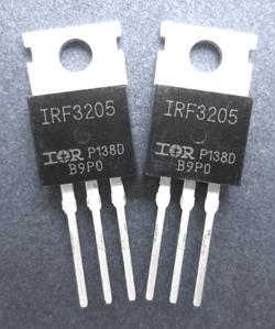
PDF IRF3205 Data sheet ( Hoja de datos )
| Número de pieza | IRF3205 | |
| Descripción | Power MOSFET ( Transistor ) | |
| Fabricantes | ART CHIP | |
| Logotipo | ||
 1. 55V, 110A, HEXFET Power MOSFET Hay una vista previa y un enlace de descarga de IRF3205 (archivo pdf) en la parte inferior de esta página. Total 7 Páginas | ||
|
No Preview Available !
IRF3205
HEXFET ® Power MOSFET
z Advanced Process Technology
z Ultra Low On-Resistance
z Dynamic dv/dt Rating
z 175 Operating Temperature
z Fast Switching
z Fully Avalanche Rated
VDSS=55V
RDS(on)=8.0mΩ
ID=110A
Description
Advanced HEXFET ® Power MOSFETs from International Rectifier utilize advanced processing techniques to achieve extremely
low on-resistance per silicon area. This benefit, combined with the fast switching speed and ruggedized device design that
HEXFET power MOSFETs are well known for, provides the designer with an extremely efficient and reliable device for use in a
wide variety of applications.
The TO-220 packages is universally preferred for all commercial-industrial applications at power dissipation levels to
approximately 50 watts. The low thermal resistance and low package cost of the TO-220 contribute to its wide acceptance
throughout the industry.
Absolute Maximum Ratings
ID@TC=25
ID@TC=100
IDM
PD @ Tc=25
Parameter
Continuous Drain Current, VGS @ 10V
Continuous Drain Current, VGS @ 10V
Pulsed Drain Current
Power Dissipation
Linear Derating Factor
VGS
IAR
EAR
dv/dt
Gate-to-Source Voltage
Avalanche Current
Repetitive Avalanche Energy
Peak Diode Recovery dv/dt
TJ
TSTG
Operating Junction and
Storage Temperature Range
Soldering Temperature, for 10 seconds
Mounting torque, 6-32 or M3 srew
Max.
110
80
390
200
1.3
±20
62
20
5.0
-55 to +175
300 (1.6mm from case)
10 Ibf•in (1.1 N•m)
Units
A
W
W/
V
A
mJ
V/ns
Thermal Resistance
Parameter
RӨJC
RӨCS
Junction-to-Case
Case-to-Sink, Flat, Greased Surface
RӨJA
Junction-to-Ambient
Typ.
-
0.50
-
Max.
0.75
-
62
Units
/W
www.artschip.com
1
1 page 
IRF3205
HEXFET ® Power MOSFET
Fig 12a. Unclamped Inductive Test Circuit
Fig 12c. Maximum Avalanche Energy
Vs. Drain Current
Fig 12b. Unclamped Inductive Waveforms
Fig 13b. Gate Charge Test Circuit
Fig 13a. Basic Gate Charge Waveform
www.artschip.com
5
5 Page | ||

| Páginas | Total 7 Páginas | |
| PDF Descargar | [ Datasheet IRF3205.PDF ] | |
Hoja de datos destacado
| Número de pieza | Descripción | Fabricantes |
| IRF320 | N-CHANNEL POWER MOSFETS | Samsung semiconductor |
| IRF320 | 2.8A and 3.3A/ 350V and 400V/ 1.8 and 2.5 Ohm/ N-Channel Power MOSFETs | Intersil Corporation |
| IRF320 | N-Channel Power MOSFETs/ 3.0 A/ 350-400 V | Fairchild Semiconductor |
| IRF320 | N-Channel MOSFET Transistor | Inchange Semiconductor |
| Número de pieza | Descripción | Fabricantes |
| SLA6805M | High Voltage 3 phase Motor Driver IC. |
Sanken |
| SDC1742 | 12- and 14-Bit Hybrid Synchro / Resolver-to-Digital Converters. |
Analog Devices |
|
DataSheet.es es una pagina web que funciona como un repositorio de manuales o hoja de datos de muchos de los productos más populares, |
| DataSheet.es | 2020 | Privacy Policy | Contacto | Buscar |