|
|
|
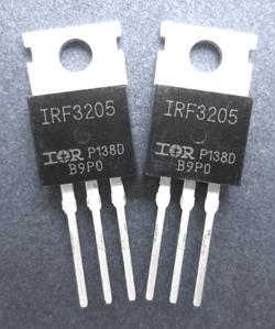
PDF IRF3205 Data sheet ( Hoja de datos )
| Número de pieza | IRF3205 | |
| Descripción | N-Channel Power MOSFET / Transistor | |
| Fabricantes | First Silicon | |
| Logotipo | ||
 1. 55V, 110A, HEXFET Power MOSFET Hay una vista previa y un enlace de descarga de IRF3205 (archivo pdf) en la parte inferior de esta página. Total 2 Páginas | ||
|
No Preview Available !
SEMICONDUCTOR
TECHNICAL DATA
N-Channel Power MOSFET (55V/120A)
Purpose
Suited for low voltage applications such as automotive,
DC/DC Converters, and high efficiency switching
for power management in portable and battery operated products
Feature
Low RDS(on),low gate charge,low Crss,fast switching.
IRF3205
Absolute maximum ratings(Ta=25℃)
Parameter
Drain-Source Voltage
Drain Current
Drain Current
Pulsed Drain Current
Gate-Source Voltage
Avalanche Current
Single Pulsed Avalanche Energy
Repetitive Avalanche Energy
Total Power Dissipation
Junction and Storage Temperature Range
Symbol
VDSS
ID(Tc=25℃)
ID(Tc=100℃)
IDM
VGSS
IAR
EAS
EAR
PD(Tc=25℃)
TJ,TSTG
Rating
55
110
80
390
±20
62
1050
20
200
-55 to 150
Unit
V
A
A
A
V
A
mJ
mJ
W
℃
1.Gate 2.Drain 3.Source
Electrical Characteristics(Ta=25℃)
Parameter
Symbol
Test Conditions
Min Typ Max Unit
Zero Gate Voltage Drain Current BVDSS VGS=0V
ID=250μA 55
V
Zero Gate Voltage Drain Current
Gate-Body Leakage Current
Forward
VDS=55V VGS=0V
IDSS VDS=44V
VGS=0V
TC=150℃
IGSS VGS=±20V VDS=0V
25 μA
250 μA
±0.1 μA
Gate Threshold Voltage
Static Drain-Source
On-Resistance
VGS(th) VDS=VGS
RDS(on) VGS=10V
ID=250μA
ID=62A
2
4V
8 mΩ
Forward Transconductance
gFS VDS=25V ID=62A
44
S
Forward On Voltage
VSD VGS=0V
IS=62A
1.3 V
Input Capacitance
Output Capacitance
Reverse Transfer Capacitance
Ciss
Coss
Crss
VDS=25V
f=1MHz
VGS=0V
3247
781
211
pF
Turn-On Delay Time
td(on)
14
Turn-On Rise Time
Turn-Off Delay Time
tr
td(off)
VDD=28V
RG=4.5Ω
ID=62A
101
ns
50
Turn-Off Fall Time
tf
65
2015. 01. 10
Revision No : 0
1/2
1 page | ||

| Páginas | Total 2 Páginas | |
| PDF Descargar | [ Datasheet IRF3205.PDF ] | |
Hoja de datos destacado
| Número de pieza | Descripción | Fabricantes |
| IRF320 | N-CHANNEL POWER MOSFETS | Samsung semiconductor |
| IRF320 | 2.8A and 3.3A/ 350V and 400V/ 1.8 and 2.5 Ohm/ N-Channel Power MOSFETs | Intersil Corporation |
| IRF320 | N-Channel Power MOSFETs/ 3.0 A/ 350-400 V | Fairchild Semiconductor |
| IRF320 | N-Channel MOSFET Transistor | Inchange Semiconductor |
| Número de pieza | Descripción | Fabricantes |
| SLA6805M | High Voltage 3 phase Motor Driver IC. |
Sanken |
| SDC1742 | 12- and 14-Bit Hybrid Synchro / Resolver-to-Digital Converters. |
Analog Devices |
|
DataSheet.es es una pagina web que funciona como un repositorio de manuales o hoja de datos de muchos de los productos más populares, |
| DataSheet.es | 2020 | Privacy Policy | Contacto | Buscar |