|
|
|
PDF 33931 Data sheet ( Hoja de datos )
| Número de pieza | 33931 | |
| Descripción | 5.0A Throttle Control H-bridge | |
| Fabricantes | Freescale Semiconductor | |
| Logotipo | ||
Hay una vista previa y un enlace de descarga de 33931 (archivo pdf) en la parte inferior de esta página. Total 26 Páginas | ||
|
No Preview Available !
Freescale Semiconductor
Technical Data
Document Number: MC33931
Rev. 4.0, 10/2012
5.0 A Throttle Control H-bridge
The 33931 is a monolithic H-Bridge Power IC in a robust thermally
enhanced package. It is designed primarily for automotive electronic
throttle control, but is applicable to any low voltage DC servo motor
control application within the current and voltage limits stated in this
specification.
33931
THROTTLE CONTROL H-BRIDGE
The 33931 H-Bridge is able to control inductive loads with currents
up to 5.0 A peak. RMS current capability is subject to the degree of
heatsinking provided to the device package. Internal peak-current
limiting (regulation) is activated at load currents above 6.5 A ±1.5 A.
Output loads can be pulse-width modulated (PWM-ed) at frequencies
up to 11 kHz. A load current feedback feature provides a proportional
(0.24% of the load current) current output suitable for monitoring by a
microcontroller’s A/D input. A Status flag output reports under-voltage,
over-current, and over-temperature fault conditions.
Two independent inputs provide polarity control of two half-bridge
totem-pole outputs. The disable inputs are provided to force the H-
bridge outputs to tri-state (high-impedance off-state).
VW SUFFIX (PB-FREE)
98ARH98330A
44-PIN HSOP
WITH PROTRUDING
HEAT SINK
EK SUFFIX (PB-FREE)
98ARL10543D
32-PIN SOICW-EP
Features
• 5.0 to 28 V continuous operation (transient operation from 5.0 to
40 V)
• 235 mΩ maximum RDS(ON) @ TJ=150 °C (each H-bridge
MOSFET)
• 3.0 V and 5.0 V TTL / CMOS logic compatible inputs
ORDERING INFORMATION
Device
(Add R2 Suffix for
Tape and Reel)
Temperature
Range (TA)
Package
MC33931VW
MC33931EK
-40 to 125°C
44 HSOP
32 SOICW-EP
• Over-current limiting (regulation) via internal constant-off-time
PWM
• Output short-circuit protection (short to VPWR or GND)
• Temperature-dependant current-limit threshold reduction
• All inputs have an internal source/sink to define the default (floating input) states
• Sleep mode with current draw < 50 µA
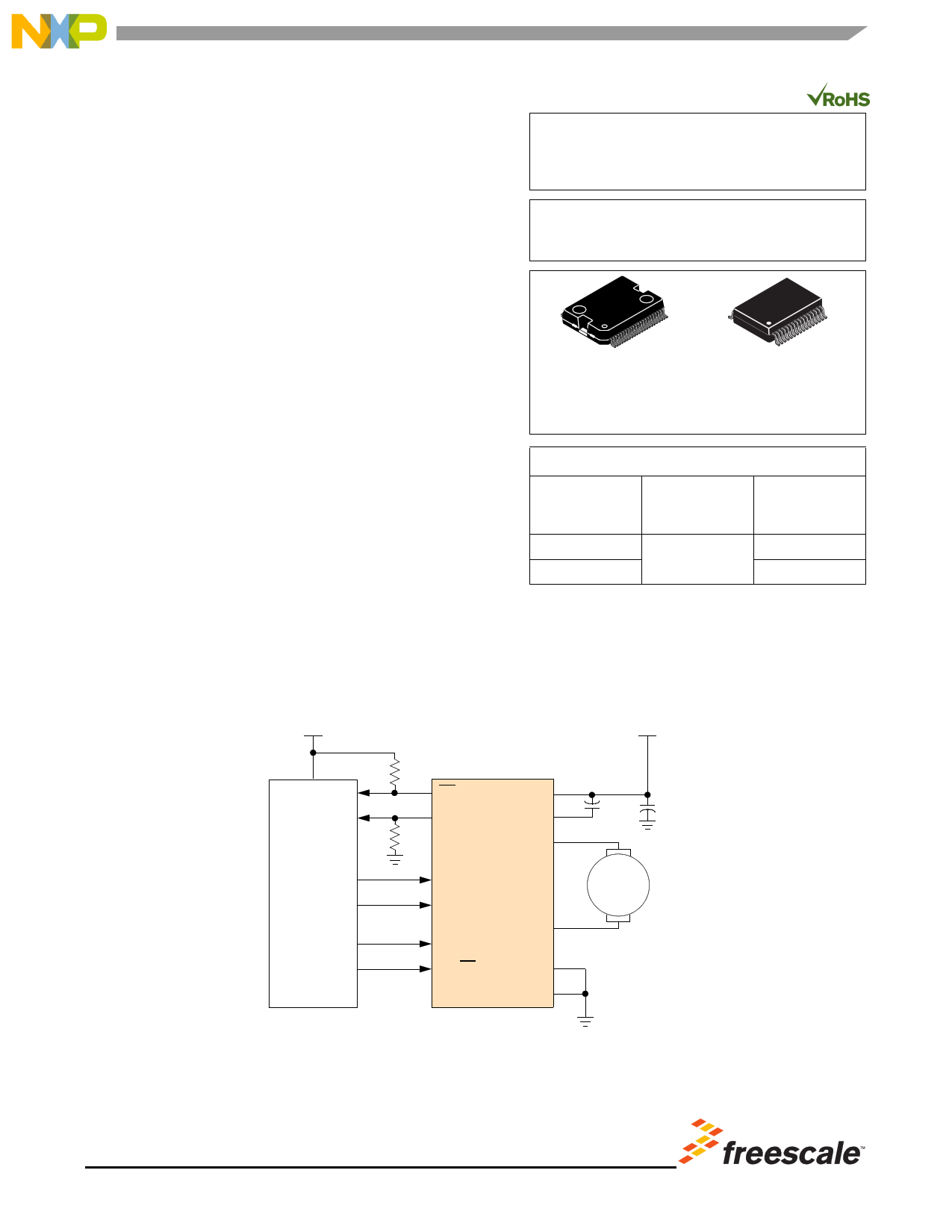
VDD
VPWR
MCU
33931
SF VPWR
FB CCP
OUT1
IN1
IN2
D1
EN/D2
OUT2
PGND
AGND
MOTOR
Figure 1. MC33931 Simplified Application Diagram
© Freescale Semiconductor, Inc., 2008-2012. All rights reserved.
1 page 
ELECTRICAL CHARACTERISTICS
MAXIMUM RATINGS
ELECTRICAL CHARACTERISTICS
MAXIMUM RATINGS
Table 2. Maximum Ratings
All voltages are with respect to ground, unless otherwise noted. Exceeding these ratings may cause a malfunction or
permanent damage to the device. These parameters are not production tested.
Ratings
Symbol
Value
Unit
ELECTRICAL RATINGS
Power Supply Voltage
Normal Operation (Steady-state)
Transient Over-voltage(1)
Logic Input Voltage(2)
SF Output(3)
Continuous Output Current(4)
ESD Voltage(5)
Human Body Model
Machine Model
Charge Device Model
Corner Pins
All Other Pins
VPWR(SS)
VPWR(T)
VIN
V SF
IOUT(CONT)
VESD1
VESD2
-0.3 to 28
-0.3 to 40
-0.3 to 7.0
-0.3 to 7.0
5.0
± 2000
± 200
±750
±500
V
V
V
A
V
THERMAL RATINGS
Storage Temperature
Operating Temperature(6)
Ambient
Junction
Peak Package Reflow Temperature During Reflow(7),(8)
Approximate Junction-to-Case Thermal Resistance (9)
TSTG
TA
TJ
TPPRT
RθJC
- 65 to 150
-40 to 125
-40 to 150
Note 8
< 1.0
°C
°C
°C
°C/W
Notes
1. Device will survive repetitive transient over-voltage conditions for durations not to exceed 500 ms @ duty cycle not to exceed 10%.
External protection is required to prevent device damage in case of a reverse battery condition.
2. Exceeding the maximum input voltage on IN1, IN2, EN/D2 or D1 may cause a malfunction or permanent damage to the device.
3. Exceeding the pull-up resistor voltage on the open drain SF pin may cause permanent damage to the device.
4. Continuous output current capability is dependent on sufficient package heatsinking to keep junction temperature ≤150°C.
5. ESD testing is performed in accordance with the Human Body Model (CZAP = 100 pF, RZAP = 1500 Ω), Machine Model (CZAP = 200 pF,
RZAP = 0 Ω), and the Charge Device Model (CDM), Robotic (CZAP = 4.0 pF).
6. The limiting factor is junction temperature, taking into account the power dissipation, thermal resistance, and heat sinking provided. Brief
non-repetitive excursions of junction temperature above 150°C can be tolerated, provided the duration does not exceed 30 seconds
maximum. (Non-repetitive events are defined as not occurring more than once in 24 hours.)
7. Pin soldering temperature limit is for 10 seconds maximum duration. Not designed for immersion soldering. Exceeding these limits may
cause malfunction or permanent damage to the device.
8. Freescale’s Package Reflow capability meets Pb-free requirements for JEDEC standard J-STD-020C. For Peak Package Reflow
Temperature and Moisture Sensitivity Levels (MSL), Go to www.freescale.com, search by part number [e.g. remove prefixes/suffixes
and enter the core ID to view all orderable parts. (i.e. MC33xxxD enter 33xxx), and review parametrics.
9. Exposed heatsink pad plus the power and ground pins comprise the main heat conduction paths. The actual RθJB (junction-to-PC board)
values will vary depending on solder thickness and composition and copper trace thickness and area. Maximum current at maximum
die temperature represents ~16 W of conduction loss heating in the diagonal pair of output MOSFETs. Therefore, the RθJA must be
<5.0 °C/W for maximum current at 70 °C ambient. Module thermal design must be planned accordingly.
Analog Integrated Circuit Device Data
Freescale Semiconductor
33931
5
5 Page 
FUNCTIONAL DESCRIPTION
INTRODUCTION
FUNCTIONAL DESCRIPTION
INTRODUCTION
Numerous protection and operational features (speed,
torque, direction, dynamic breaking, PWM control, and
closed-loop control) make the 33931 a very attractive, cost-
effective solution for controlling a broad range of small DC
motors. The 33931 outputs are capable of supporting peak
DC load currents of up to 5.0 A from a 28 V VPWR source. An
internal charge pump and gate drive circuitry are provided
that can support external PWM frequencies up to 11 kHz.
The 33931 has an analog feedback (current mirror) output
pin (the FB pin) that provides a constant-current source
ratioed to the active high side MOSFETs’ current. This can be
used to provide “real time” monitoring of output current to
facilitate closed-loop operation for motor speed/torque
control, or for the detection of open load conditions.
Two independent inputs, IN1 and IN2, provide control of
the two totem-pole half-bridge outputs. Two independent
disable inputs, D1 and EN/D2, provide the means to force the
H-bridge outputs to a high-impedance state (all H-Bridge
switches OFF). The EN/D2 pin also controls an enable
function that allows the IC to be placed in a power-conserving
Sleep mode.
The 33931 has output current limiting (via constant OFF-
time PWM current regulation), output short-circuit detection
with latch-OFF, and over-temperature detection with latch-
OFF. Once the device is latched-OFF due to a fault condition,
either of the Disable inputs (D1 or EN/D2), or VPWR must be
“toggled” to clear the status flag.
Current limiting (Load Current Regulation) is
accomplished by a constant-OFF time PWM method using
current limit threshold triggering. The current limiting scheme
is unique in that it incorporates a junction temperature-
dependent current limit threshold. This means that the
current limit threshold is “reduced to around 4.2 A” as the
junction temperature increases above 160 °C. When the
temperature is above 175 °C, over-temperature shutdown
(latch-OFF) will occur. This combination of features allows
the device to continue operating for short periods of time (<30
seconds) with unexpected loads, while still retaining
adequate protection for both the device and the load.
FUNCTIONAL PIN DESCRIPTION
POWER GROUND AND ANALOG GROUND
(PGND AND AGND)
The power and analog ground pins should be connected
together with a very low-impedance connection.
POSITIVE POWER SUPPLY (VPWR)
VPWR pins are the power supply inputs to the device. All
VPWR pins must be connected together on the printed circuit
board with as short as possible traces, offering as low an
impedance as possible between pins.
STATUS FLAG (SF)
This pin is the device fault status output. This output is an
active LOW open drain structure requiring a pull-up resistor
to VDD. The maximum VDD is <7.0 V. Refer to Table 5, for the
SF Output status definition.
INPUT 1,2 AND DISABLE INPUT 1
(IN1, IN2, AND D1)
These pins are input control pins used to control the
outputs. These pins are 3.0 V/5.0 V CMOS-compatible
inputs with hysteresis. IN1 and IN2 independently control
OUT1 and OUT2, respectively. D1 input is used to tri-state
disable the H-bridge outputs.
When D1 is SET (D1 = logic HIGH) in the disable state,
outputs OUT1 and OUT2 are both tri-state disabled; however,
the rest of the device circuitry is fully operational and the
supply IPWR(STANDBY) current is reduced to a few mA. Refer
to Table 3, Static Electrical Characteristics, page 6.
H-BRIDGE OUTPUT (OUT1, OUT2)
These pins are the outputs of the H-Bridge with integrated
free-wheeling diodes. The bridge output is controlled using
the IN1, IN2, D1, and EN/D2 inputs. The outputs have PWM
current limiting above the ILIM threshold. The outputs also
have thermal shutdown (tri-state latch-OFF) with hysteresis
as well as short-circuit latch-OFF protection.
A disable timer (time tB) is incorporated to distinguish
between load currents that are higher than the ILIM threshold
and short-circuit currents. This timer is activated at each
output transition.
CHARGE PUMP CAPACITOR (CCP)
This pin is the charge pump output pin and connection for
the external charge pump reservoir capacitor. The allowable
value is from 30 nF to 100 nF. This capacitor must be
connected from the CCP pin to the VPWR pin. The device
cannot operate properly without the external reservoir
capacitor.
ENABLE INPUT/DISABLE INPUT 2 (EN/D2)
The EN/D2 pin performs the same function as D1 pin,
when it goes to a logic LOW the outputs are immediately tri-
stated. It is also used to place the device in a Sleep mode so
as to consume very low currents. When the EN/D2 pin
voltage is a logic LOW state, the device is in the Sleep mode.
Analog Integrated Circuit Device Data
Freescale Semiconductor
33931
11
11 Page | ||
| Páginas | Total 26 Páginas | |
| PDF Descargar | [ Datasheet 33931.PDF ] | |
Hoja de datos destacado
| Número de pieza | Descripción | Fabricantes |
| 33931 | 5.0A Throttle Control H-bridge | Freescale Semiconductor |
| 33932 | 5.0A Throttle Control H-Bridge | Freescale Semiconductor |
| 33937A | Three phase field effect transistor pre-driver | NXP Semiconductors |
| Número de pieza | Descripción | Fabricantes |
| SLA6805M | High Voltage 3 phase Motor Driver IC. |
Sanken |
| SDC1742 | 12- and 14-Bit Hybrid Synchro / Resolver-to-Digital Converters. |
Analog Devices |
|
DataSheet.es es una pagina web que funciona como un repositorio de manuales o hoja de datos de muchos de los productos más populares, |
| DataSheet.es | 2020 | Privacy Policy | Contacto | Buscar |