|
|
|
PDF MBM29DL64DF-70 Data sheet ( Hoja de datos )
| Número de pieza | MBM29DL64DF-70 | |
| Descripción | FLASH MEMORY CMOS 64M (8 M x 8/4 M x 16) BIT | |
| Fabricantes | Fujitsu | |
| Logotipo | ||
Hay una vista previa y un enlace de descarga de MBM29DL64DF-70 (archivo pdf) en la parte inferior de esta página. Total 30 Páginas | ||
|
No Preview Available !
FUJITSU SEMICONDUCTOR
DATA SHEET
DS05-20905-1E
FLASH MEMORY
CMOS
64 M (8 M × 8/4 M × 16) BIT
Dual Operation
MBM29DL64DF-70
s DESCRIPTION
MBM29DL64DF is a 64 M-bit, 3.0 V-only Flash memory organized as 8 Mbytes of 8 bits each or 4 M words of 16
bits each. The device comes in 48-pin TSOP (1) and 48-ball FBGA packages. This device is designed to be
programmed in system with 3.0 V VCC supply. 12.0 V VPP and 5.0 V VCC are not required for write or erase operations.
The device can also be reprogrammed in standard EPROM programmers.
The device is organized into four physical banks : Bank A, Bank B, Bank C and Bank D, which are considered to
be four separate memory arrays operations. This device is the almost identical to Fujitsu’s standard 3 V only Flash
memories, with the additional capability of allowing a normal non-delayed read access from a non-busy bank of
the array while an embedded write (either a program or an erase) operation is simultaneously taking place on the
other bank.
s PRODUCT LINE UP
(Continued)
Part No.
Power Supply Voltage VCC (V)
Max Address Access Time (ns)
Max CE Access Time (ns)
Max OE Access Time (ns)
MBM29DL64DF-70
3.0
V
+0.6 V
−0.3 V
70
70
30
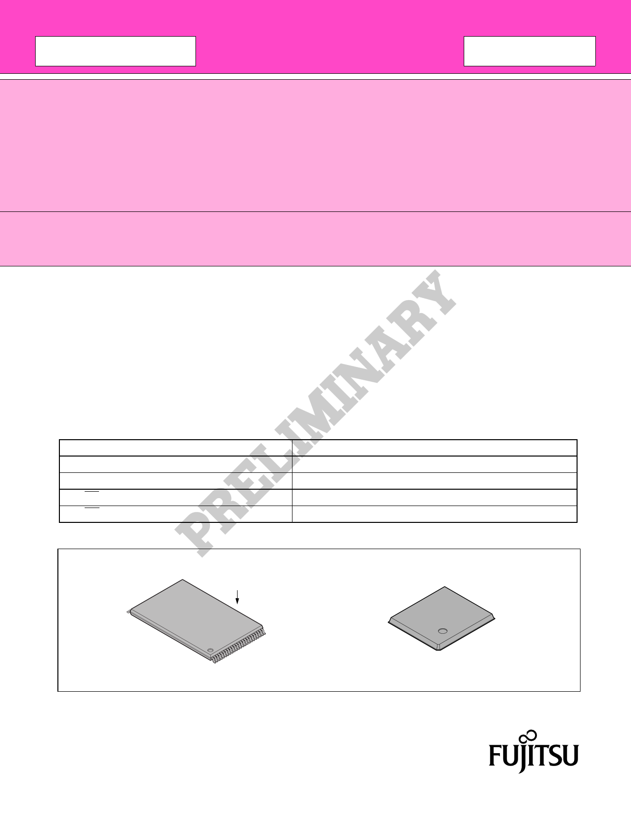
s PACKAGES
48-pin plastic TSOP (1)
48-ball plastic FBGA
Marking Side
(FPT-48P-M19)
(BGA-48P-M13)
1 page 
s PIN ASSIGNMENTS
A15
A14
A13
A12
A11
A10
A9
A8
A19
A20
WE
RESET
A21
WP/ACC
RY/BY
A18
A17
A7
A6
A5
A4
A3
A2
A1
1
2
3
4
5
6
7
8
9
10
11
12
13
14
15
16
17
18
19
20
21
22
23
24
MBM29DL64DF-70
TSOP (1)
(Marking Side)
Normal Bend
(FPT-48P-M19)
48 A16
47 BYTE
46 VSS
45 DQ15/A-1
44 DQ7
43 DQ14
42 DQ6
41 DQ13
40 DQ5
39 DQ12
38 DQ4
37 VCC
36 DQ11
35 DQ3
34 DQ10
33 DQ2
32 DQ9
31 DQ1
30 DQ8
29 DQ0
28 OE
27 VSS
26 CE
25 A0
(Continued)
5
5 Page 
MBM29DL64DF-70
(Continued)
Command
Sequence
Bus
Write
Cycles
Req’d
First Bus Second Bus
Write Cycle Write Cycle
Addr. Data Addr. Data
Third Bus
Write Cycle
Addr. Data
Fourth Bus
Read/Write
Cycle
Addr. Data
Fifth Bus
Write Cycle
Addr. Data
Sixth Bus
Write Cycle
Addr. Data
HiddenROM Word
Program *9, *10 Byte
4
555h
AAAh
AAh
2AAh
555h
55h
555h
AAAh
A0h
(HRA)
PA
PD
HiddenROM
Exit *10
Word
Byte
4
555h
2AAh
(HRBA)
555h
AAh 55h 90h XXXh 00h
AAAh
555h
(HRBA)
AAAh
*1 : Command combinations not described in “MBM29DL64DF Command Definitions” are illegal.
*2 : Both of these reset commands are equivalent.
*3 : Erase Suspend and Erase Resume command are valid only during a sector erase operations.
*4 : This command is valid during Fast Mode.
*5 : The Reset from Fast mode command is required to return to the Read mode when the device is in Fast mode.
*6 : This command is valid while RESET = VID (except during HiddenROM mode) .
*7 : Sector Group Address (SGA) with (A6, A3, A2, A1, A0) = (0, 0, 0, 1, 0) .
*8 : The valid address are A6 to A0.
*9 : The HiddenROM Entry command is required prior to the HiddenROM programming.
*10 : This command is valid during HiddenROM mode.
*11 : The data “F0h” is also acceptable.
*12 : Fourth bus cycle becomes read cycle.
Notes : • Address bits A21 to A11 = X = “H” or “L” for all address commands except or Program Address (PA) , Sector
Address (SA) , Bank Address (BA) and Sector Group Address (SPA) .
• Bus operations are defined in “MBM29DL64DF User Bus Operations (BYTE = VIH) ” and “MBM29DL64DF
User Bus Operations (BYTE = VIL) ”.
• RA = Address of the memory location to be read
IA = Autoselect read address that sets both the bank address specified at (A21, A20, A19) and all the
other A6, A3, A2, A1, A0 and (A-1) .
PA = Address of the memory location to be programmed
Addresses are latched on the falling edge of the write pulse.
SA = Address of the sector to be erased. The combination of A21, A20, A19, A18, A17, A16, A15, A14, A13 and
A12 will uniquely select any sector.
BA = Bank Address. Address setted by A21, A20, A19 will select Bank A, Bank B, Bank C and Bank D.
• RD = Data read from location RA during read operation.
ID = Device code/manufacture code for the address located by IA.
PD = Data to be programmed at location PA. Data is latched on the rising edge of write pulse.
• SPA = Sector group address to be protected. Set sector group address and (A6, A3, A2, A1, A0) =
(0, 0, 0, 1, 0) .
• SGA = Sector Group Address. The combination of A21 to A12 will uniquely select any sector group.
SD = Sector group protection verify data. Output 01h at protected sector group addresses and output
00h at unprotected sector group addresses.
• HRA = Address of the HiddenROM area
Word Mode : 000000h to 00007Fh
Byte Mode : 000000h to 0000FFh
• HRBA = Bank Address of the HiddenROM area (A21 = A20 = A19 = VIL)
• The system should generate the following address patterns :
Word Mode : 555h or 2AAh to addresses A10 to A0
Byte Mode : AAAh or 555h to addresses A10 to A0, and A-1
• Both Read/Reset commands are functionally equivalent, resetting the device to the read mode.
11
11 Page | ||
| Páginas | Total 30 Páginas | |
| PDF Descargar | [ Datasheet MBM29DL64DF-70.PDF ] | |
Hoja de datos destacado
| Número de pieza | Descripción | Fabricantes |
| MBM29DL64DF-70 | FLASH MEMORY CMOS 64M (8 M x 8/4 M x 16) BIT | Fujitsu |
| Número de pieza | Descripción | Fabricantes |
| SLA6805M | High Voltage 3 phase Motor Driver IC. |
Sanken |
| SDC1742 | 12- and 14-Bit Hybrid Synchro / Resolver-to-Digital Converters. |
Analog Devices |
|
DataSheet.es es una pagina web que funciona como un repositorio de manuales o hoja de datos de muchos de los productos más populares, |
| DataSheet.es | 2020 | Privacy Policy | Contacto | Buscar |