|
|
|
PDF LTM4650 Data sheet ( Hoja de datos )
| Número de pieza | LTM4650 | |
| Descripción | Dual 25A or Single 50A DC/DC uModule Regulator | |
| Fabricantes | Linear Technology | |
| Logotipo | ||
Hay una vista previa y un enlace de descarga de LTM4650 (archivo pdf) en la parte inferior de esta página. Total 30 Páginas | ||
|
No Preview Available !
FEATURES
nn Dual 25A or Single 50A Output
nn Input Voltage Range: 4.5V to 15V
nn Output Voltage Range: 0.6V to 1.8V
nn ±1.5% Maximum Total DC Output Error Over Line,
Load and Temperature
nn Differential Remote Sense Amplifier
nn Current Mode Control/Fast Transient Response
nn Adjustable Switching Frequency
nn Frequency Synchronization
nn Overcurrent Foldback Protection
nn Multiphase Parallel Current Sharing with Multiple
LTM4650s Up to 300A
nn Internal Temperature Monitor
nn Pin Compatible with the LTM4620 (Dual 13A, Single
26A) and LTM4630 (Dual 18A, Single 36A)
nn Selectable Burst Mode® Operation
nn Soft-Start/Voltage Tracking
nn Output Overvoltage Protection
nn 16mm × 16mm × 5.01mm BGA Package
APPLICATIONS
nn Processor, ASIC and FPGA Core Power
nn Telecom and Networking Equipment
nn Storage and ATCA Cards
nn Industrial Equipment
LTM4650
Dual 25A or Single 50A
DC/DC µModule Regulator
DESCRIPTION
The LTM®4650 is a dual 25A or single 50A output switch-
ing mode step-down DC/DC µModule® (power module)
regulator. Included in the package are the switching
controllers, power FETs, inductors, and all supporting
components. Operating from an input voltage range of
4.5V to 15V, the LTM4650 supports two outputs each
with an output voltage range of 0.6V to 1.8V, each set by a
single external resistor. Its high efficiency design delivers
up to 25A continuous current for each output. Only a few
input and output capacitors are needed. The LTM4650 is
pin compatible with the LTM4620 (dual 13A, single 26A)
and the LTM4630 (dual 18A, single 36A).
The device supports frequency synchronization, multi-
phase operation, Burst Mode operation and output voltage
tracking for supply rail sequencing and has an onboard
temperature diode for device temperature monitoring. High
switching frequency and a current mode architecture enable
a very fast transient response to line and load changes
without sacrificing stability.
Fault protection features include overvoltage and
overcurrent protection. The LTM4650 is offered in a
16mm × 16mm × 5.01mm BGA package.
L, LT, LTC, LTM, Linear Technology, the Linear logo, µModule, Burst Mode and PolyPhase are
registered trademarks of Linear Technology Corporation. All other trademarks are the property
of their respective owners. Protected by U.S. Patents, including 5481178, 5705919, 5929620,
6100678, 6144194, 6177787, 6304066 and 6580258. Other patents pending.
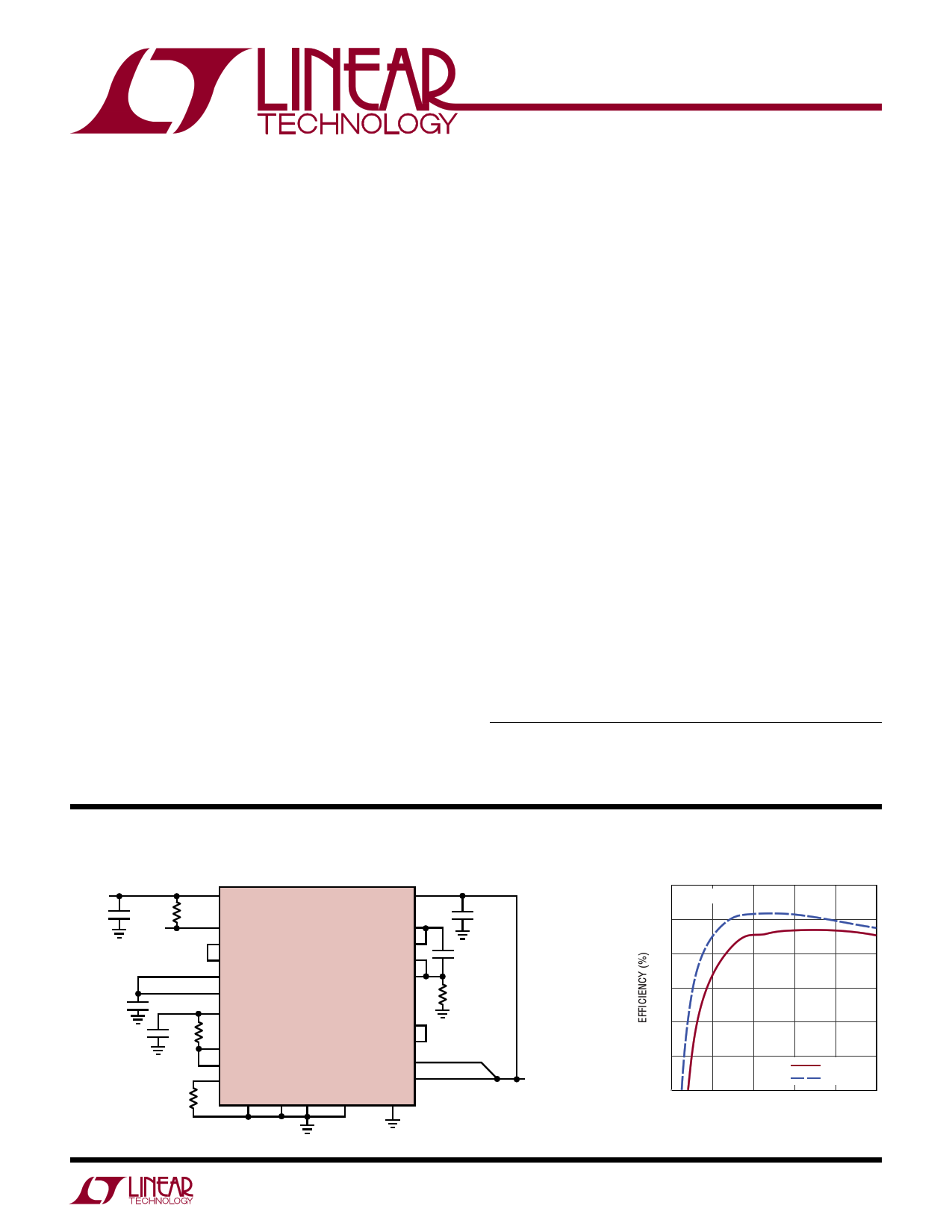
TYPICAL APPLICATION
50A, 1.2V Output DC/DC µModule Regulator
VIN
4.5V TO
15V
22µF
* 25V
×4
120k
VIN
TEMP
VOUT1
DIFFOUT
RUN1
VOUTS2
RUN2
TRACK1
LTM4650
VFB1
VFB2
PINS NOT USED
IN THIS CIRCUIT:
CLKOUT
EXTVCC
SW1
SW2
VOUTS1
0.1µF
4.7µF
TRACK2
INTVCC
10k
PGOOD1
COMP1
COMP2
PGOOD2
DIFFP
fSET VOUT2
121k PHASMD SGND GND MODE_PLLIN DIFFN
220µF
CERAMIC
4V
×8
470pF
60.4k
VOUT2
1.2V
50A
4650 TA01a
For more information www.linear.com/LTM4650
1.2VOUT Efficiency vs IOUT
95
fSW = 500KHz
90
85
80
75
70 VIN = 12V
VIN = 5V
65
0 10 20 30 40 50
LOAD CURRENT (A)
4650 TA01b
4650fb
1
1 page 
LTM4650
E LECTRICAL CHARACTERISTICS The l denotes the specifications which apply over the specified internal
operating temperature range. Specified
unless otherwise noted. Per the typical
as each individual output
application in Figure 22.
channel.
TA
=
25°C
(Note
2),
VIN
=
12V
and
VRUN1,
VRUN2
at
5V
SYMBOL
PARAMETER
CONDITIONS
MIN TYP MAX UNITS
Differential Amplifier
AV Differential
Amplifier
Gain
1 V/V
RIN
VOS
PSRR Differential
Amplifier
Input Resistance
Input Offset Voltage
Power Supply Rejection Ratio
Measured at DIFFP Input
VDIFFP = VDIFFOUT = 1.5V, IDIFFOUT = 100µA
5V < VIN < 15V
80
3
90
kΩ
mV
dB
ICL
VOUT(MAX)
GBW
Maximum Output Current
Maximum Output Voltage
Gain Bandwidth Product
IDIFFOUT = 300µA
INTVCC – 1.4
3
3
mA
V
MHz
VTEMP
TC
Diode Connected PNP
Temperature Coefficient
I = 100µA
0.6 V
l –2.2 mV/C
Note 1: Stresses beyond those listed under Absolute Maximum Ratings
may cause permanent damage to the device. Exposure to any Absolute
Maximum Rating condition for extended periods may affect device
reliability and lifetime.
Note 2: The LTM4650 is tested under pulsed load conditions such that
TJ ≈ TA. The LTM4650E is guaranteed to meet specifications from
0°C to 125°C internal temperature. Specifications over the –40°C to
125°C internal operating temperature range are assured by design,
characterization and correlation with statistical process controls. The
LTM4650I is guaranteed over the full –40°C to 125°C internal operating
temperature range. Note that the maximum ambient temperature
consistent with these specifications is determined by specific operating
conditions in conjunction with board layout, the rated package thermal
impedance and other environmental factors.
Note 3: Two outputs are tested separately and the same testing condition
is applied to each output.
Note 4: LTM4650 device is designed to operate from 400kHz to 750kHz.
Note 5: These parameters are tested at wafer sort.
Note 6: See output current derating curves for different VIN, VOUT and TA.
Note 7: Total DC output voltage error includes all errors over temperature:
line and load regulation as well as the tolerance of the integrated top
feedback resistor.
For more information www.linear.com/LTM4650
4650fb
5
5 Page 
LTM4650
OPERATION
Power Module Description
The LTM4650 is a dual-output standalone nonisolated
switching mode DC/DC power supply. It can provide two
25A outputs with few external input and output capacitors
and setup components. This module provides precisely
regulated output voltages programmable via external
resistors from 0.6VDC to 1.8VDC over 4.5V to 15V input
voltages. The typical application schematic is shown in
Figure 22.
The LTM4650 has dual integrated constant-frequency cur-
rent mode regulators and built-in power MOSFET devices
with fast switching speed. The typical switching frequency
is from 400kHz to 600kHz depending on output voltage. For
switching-noise sensitive applications, it can be externally
synchronized from 400kHz to 780kHz. A resistor can be
used to program a free run frequency on the FSET pin.
See the Applications Information section.
With current mode control and internal feedback loop
compensation, the LTM4650 module has sufficient stabil-
ity margins and good transient performance with a wide
range of output capacitors, even with all ceramic output
capacitors.
Current mode control provides cycle-by-cycle fast current
limit and foldback current limit in an overcurrent condition.
Internal overvoltage and undervoltage comparators pull
the open-drain PGOOD outputs low if the output feedback
voltage exits a ±10% window around the regulation point.
As the output voltage exceeds 10% above regulation, the
bottom MOSFET will turn on to clamp the output voltage.
The top MOSFET will be turned off. This overvoltage protect
is feedback voltage referred.
Pulling the RUN pins below 1.1V forces the regulators into
a shutdown state, by turning off both MOSFETs. The TRACK
pins are used for programming the output voltage ramp and
voltage tracking during start-up or used for soft-starting
the regulator. See the Applications Information section.
The LTM4650 is internally compensated to be stable over all
operating conditions. Table 4 provides a guide line for input
and output capacitances for several operating conditions.
The Linear Technology µModule Power Design Tool will be
provided for transient and stability analysis. The VFB pin is
used to program the output voltage with a single external
resistor to ground. A differential remote sense amplifier is
available for sensing the output voltage accurately on one
of the outputs at the load point, or in parallel operation
sensing the output voltage at the load point.
Multiphase operation can be easily employed with the
MODE_PLLIN, PHASMD, and CLKOUT pins. Up to
12 phases can be cascaded to run simultaneously with
respect to each other by programming the PHASMD pin to
different levels. See the Applications Information section.
High efficiency at light loads can be accomplished with
selectable Burst Mode operation or pulse-skipping opera-
tion using the MODE_PLLIN pin. These light load features
will accommodate battery operation. Efficiency graphs are
provided for light load operation in the Typical Performance
Characteristics section. See the Applications Information
section for details.
A general purpose temperature diode is included inside
the module to monitor the temperature of the module. See
the Applications Information section for details.
The switch pins are available for functional operation
monitoring and a resistor-capacitor snubber circuit can
be careful placed on the switch pin to ground to dampen
any high frequency ringing on the transition edges. See
the Applications Information section for details.
For more information www.linear.com/LTM4650
4650fb
11
11 Page | ||
| Páginas | Total 30 Páginas | |
| PDF Descargar | [ Datasheet LTM4650.PDF ] | |
Hoja de datos destacado
| Número de pieza | Descripción | Fabricantes |
| LTM4650 | Dual 25A or Single 50A DC/DC uModule Regulator | Linear Technology |
| LTM4650-1 | Dual 25A or Single 50A uModule Regulator | Linear Technology |
| LTM4650A | Dual 25A or Single 50A DC/DC uModule Regulator | Linear Technology |
| LTM4650A-1 | Dual 25A or Single 50A DC/DC uModule Regulator | Linear Technology |
| Número de pieza | Descripción | Fabricantes |
| SLA6805M | High Voltage 3 phase Motor Driver IC. |
Sanken |
| SDC1742 | 12- and 14-Bit Hybrid Synchro / Resolver-to-Digital Converters. |
Analog Devices |
|
DataSheet.es es una pagina web que funciona como un repositorio de manuales o hoja de datos de muchos de los productos más populares, |
| DataSheet.es | 2020 | Privacy Policy | Contacto | Buscar |