|
|
|
PDF K4E171611C Data sheet ( Hoja de datos )
| Número de pieza | K4E171611C | |
| Descripción | 1M x 16Bit CMOS Dynamic RAM | |
| Fabricantes | Samsung | |
| Logotipo | ||
Hay una vista previa y un enlace de descarga de K4E171611C (archivo pdf) en la parte inferior de esta página. Total 30 Páginas | ||
|
No Preview Available !
K4E171611C, K4E151611C
K4E171612C, K4E151612C
CMOS DRAM
1M x 16Bit CMOS Dynamic RAM with Extended Data Out
DESCRIPTION
This is a family of 1,048,576 x 16 bit Extended Data Out CMOS DRAMs. Extended Data Out Mode offers high speed random access of
memory cells within the same row, so called Hyper Page Mode. Power supply voltage (+5.0V or +3.3V), refresh cycle (1K Ref. or 4K
Ref.), access time (-45, -50 or -60), power consumption(Normal or Low power) and package type(SOJ or TSOP-II) are optional features
of this family. All of this family have CAS-before-RAS refresh, RAS-only refresh and Hidden refresh capabilities. Furthermore, Self-
refresh operation is available in L-version. This 1Mx16 EDO Mode DRAM family is fabricated using Samsung′ s advanced CMOS pro-
cess to realize high band-width, low power consumption and high reliability. It may be used as graphic memory unit for microcomputer,
personal computer and portable machines.
FEATURES
• Part Identification
- K4E171611C-J(T)(5V, 4K Ref.)
- K4E151611C-J(T) (5V, 1K Ref.)
- K4E171612C-J(T)(3.3V, 4K Ref.)
- K4E151612C-J(T)(3.3V, 1K Ref.)
• Active Power Dissipation
Speed
-45
-50
-60
3.3V
4K 1K
360 540
324 504
288 468
Unit : mW
5V
4K 1K
550 825
495 770
440 715
• Extended Data Out Mode operation
(Fast Page Mode with Extended Data Out)
• 2 CAS Byte/Word Read/Write operation
• CAS-before-RAS refresh capability
• RAS-only and Hidden refresh capability
• Self-refresh capability (L-ver only)
• TTL(5V)/LVTTL(3.3V) compatible inputs and outputs
• Early Write or output enable controlled write
• JEDEC Standard pinout
• Available in plastic SOJ 400mil and TSOP(II) packages
• Single +5V±10% power supply (5V product)
• Single +3.3V±0.3V power supply (3.3V product)
• Refresh Cycles
Part
NO.
K4E171611C
K4E171612C
K4E151611C
K4E151612C
VCC
5V
3.3V
5V
3.3V
Refresh Refresh period
cycle Normal L-ver
4K 64ms
128ms
1K 16ms
• Performance Range
Speed
-45
-50
-60
tRAC
45ns
50ns
60ns
tCAC
13ns
15ns
17ns
tRC
69ns
84ns
104ns
tHPC
16ns
20ns
25ns
Remark
5V/3.3V
5V/3.3V
5V/3.3V
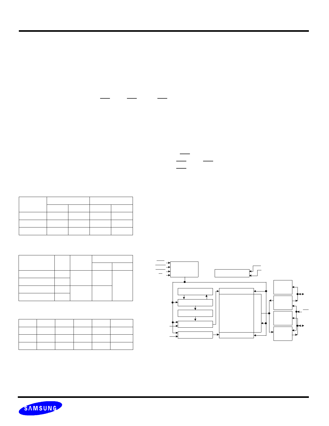
FUNCTIONAL BLOCK DIAGRAM
RAS
UCAS
LCAS
W
A0-A11
(A0 - A9)*1
A0 - A7
(A0 - A9)*1
Control
Clocks
VBB Generator
Refresh Timer
Refresh Control
Refresh Counter
Row Address Buffer
Col. Address Buffer
Row Decoder
Memory Array
1,048,576 x16
Cells
Column Decoder
Vcc
Vss
Lower
Data in
Buffer
Lower
Data out
Buffer
Upper
Data in
Buffer
Upper
Data out
Buffer
Note) *1 : 1K Refresh
DQ0
to
DQ7
OE
DQ8
to
DQ15
SAMSUNG ELECTRONICS CO., LTD. reserves the right to
change products and specifications without notice.
www.BDTIC.com/SAMSUNG
1 page 
K4E171611C, K4E151611C
K4E171612C, K4E151612C
CAPACITANCE (TA=25°C, VCC=5V or 3.3V, f=1MHz)
Parameter
Symbol
Input capacitance [A0 ~ A11]
CIN1
Input capacitance [RAS, UCAS, LCAS, W, OE]
CIN2
Output capacitance [DQ0 - DQ15]
CDQ
Min
-
-
-
CMOS DRAM
Max
5
7
7
Units
pF
pF
pF
AC CHARACTERISTICS (0°C≤TA≤70°C, See note 1,2)
Test condition (5V device) : VCC=5.0V±10%, Vih/Vil=2.4/0.8V, Voh/Vol=2.0/0.8V
Test condition (3.3V device) : VCC=3.3V±0.3V, Vih/Vil=2.2/0.7V, Voh/Vol=2.0/0.8V
Parameter
Symbol
-45
Min Max
-50
Min Max
Random read or write cycle time
tRC 79
84
Read-modify-write cycle time
tRWC
105
115
Access time from RAS
tRAC
45 50
Access time from CAS
tCAC
14 15
Access time from column address
tAA
23/*20
25
CAS to output in Low-Z
tCLZ
3
3
Output buffer turn-off delay from CAS
tCEZ
3 13 3 13
OE to output in Low-Z
Transition time (rise and fall)
tOLZ
3
3
tT 2 50 2 50
RAS precharge time
tRP 30
30
RAS pulse width
tRAS
45 10K 50 10K
RAS hold time
CAS hold time
tRSH
tCSH
13
36
13
40
CAS pulse width
tCAS
7 / *6.5 10K
8 10K
RAS to CAS delay time
tRCD
19 31 20 35
RAS to column address delay time
CAS to RAS precharge time
tRAD
tCRP
14 22 15 25
55
Row address set-up time
tASR
0
0
Row address hold time
tRAH
9
10
Column address set-up time
Column address hold time
tASC
tCAH
0
7
0
8
Column address to RAS lead time
tRAL
23
25
Read command set-up time
tRCS
0
0
Read command hold time referenced to CAS
Read command hold time referenced to RAS
tRCH
tRRH
0
0
0
0
Write command hold time
tWCH
8
10
Write command pulse width
tWP 8
10
Write command to RAS lead time
tRWL
10
13
Write command to CAS lead time
* KM416C1204CT-45 (5V, 1K Refresh) only
tCWL
7
8
-60
Min Max
104
140
60
17
30
3
3 15
3
2 50
40
60 10K
17
50
10 10K
20 43
15 30
5
0
10
0
10
30
0
0
0
10
10
15
10
Units Notes
ns
ns
ns 3,4,10
ns 3,4,5
ns 3,10
ns 3
ns 6,19
ns 3
ns 2
ns
ns
ns
ns
ns 18
ns 4
ns 10
ns
ns
ns
ns 11
ns 11
ns
ns
ns 8
ns 8
ns
ns
ns
ns 14
www.BDTIC.com/SAMSUNG
5 Page 
K4E171611C, K4E151611C
K4E171612C, K4E151612C
UPPER BYTE READ CYCLE
NOTE : DIN = OPEN
VIH -
RAS
VIL -
VIH -
UCAS
VIL -
VIH -
LCAS
VIL -
VIH -
A
VIL -
VIH -
W
VIL -
VIH -
OE
VIL -
DQ0 ~ DQ7
VOH -
VOL -
DQ8 ~ DQ15
VOH -
VOL -
tRAS
tRC
tCRP
tRCD
tCSH
tRSH
tCAS
tCRP
tRAD
tASR tRAH
ROW
ADDRESS
tASC
tRCS
tCAH
COLUMN
ADDRESS
tRAL
tRAC
OPEN
tAA
tOEA
tOLZ
OPEN
tCAC
tCLZ
CMOS DRAM
tRP
tCRP
tRPC
tRRH
tRCH
tCEZ
tOEZ
DATA-OUT
Don′t care
Undefined
www.BDTIC.com/SAMSUNG
11 Page | ||
| Páginas | Total 30 Páginas | |
| PDF Descargar | [ Datasheet K4E171611C.PDF ] | |
Hoja de datos destacado
| Número de pieza | Descripción | Fabricantes |
| K4E171611C | 1M x 16Bit CMOS Dynamic RAM | Samsung |
| K4E171611D | 1M x 16Bit CMOS Dynamic RAM with Extended Data Out | Samsung |
| Número de pieza | Descripción | Fabricantes |
| SLA6805M | High Voltage 3 phase Motor Driver IC. |
Sanken |
| SDC1742 | 12- and 14-Bit Hybrid Synchro / Resolver-to-Digital Converters. |
Analog Devices |
|
DataSheet.es es una pagina web que funciona como un repositorio de manuales o hoja de datos de muchos de los productos más populares, |
| DataSheet.es | 2020 | Privacy Policy | Contacto | Buscar |