|
|
|
PDF EMB20P03G Data sheet ( Hoja de datos )
| Número de pieza | EMB20P03G | |
| Descripción | P-Channel Logic Level Enhancement Mode Field Effect Transistor | |
| Fabricantes | Excelliance MOS | |
| Logotipo | ||
Hay una vista previa y un enlace de descarga de EMB20P03G (archivo pdf) en la parte inferior de esta página. Total 5 Páginas | ||
|
No Preview Available !
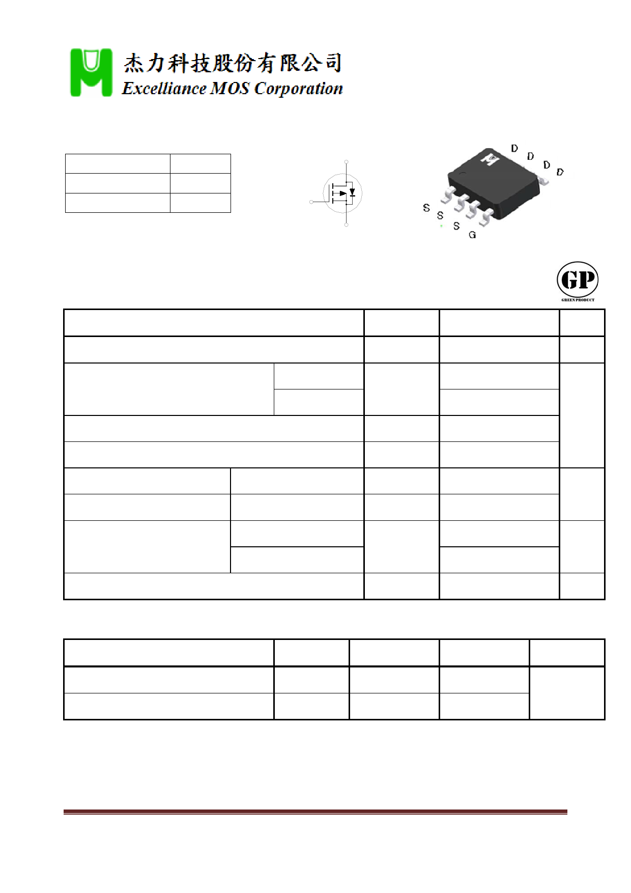
P‐Channel Logic Level Enhancement Mode Field Effect Transistor
Product Summary:
BVDSS
‐30V
D
RDSON (MAX.)
20mΩ
ID
‐10A
G
UIS, Rg 100% Tested
S
Pb‐Free Lead Plating & Halogen Free
ABSOLUTE MAXIMUM RATINGS (TA = 25 °C Unless Otherwise Noted)
PARAMETERS/TEST CONDITIONS
SYMBOL
EMB20P03G
LIMITS
UNIT
Gate‐Source Voltage
Continuous Drain Current
Pulsed Drain Current1
TC = 25 °C
TC = 100 °C
Avalanche Current
Avalanche Energy
Repetitive Avalanche Energy2
L = 0.1mH, ID=‐10A, RG=25Ω
L = 0.05mH
Power Dissipation
TA = 25 °C
TA = 100 °C
Operating Junction & Storage Temperature Range
VGS
ID
IDM
IAS
EAS
EAR
PD
Tj, Tstg
±25
‐10
‐8
‐40
‐15
5
2.5
2.5
1
‐55 to 150
V
A
mJ
W
°C
100% UIS testing in condition of VD=‐15V, L=0.1mH, VG=‐10V, IL=‐10A, Rated VDS=‐30V P‐CH
THERMAL RESISTANCE RATINGS
THERMAL RESISTANCE
SYMBOL
TYPICAL
MAXIMUM
UNIT
Junction‐to‐Case
RJC
Junction‐to‐Ambient3
RJA
1Pulse width limited by maximum junction temperature.
2Duty cycle 1%
350°C / W when mounted on a 1 in2 pad of 2 oz copper.
25
°C / W
50
2013/9/18
p.1
1 page 
10
I D = ‐ 10A
8
6
4
Gate Charge Characteristics
VD S = ‐ 5V
‐ 15V
‐ 10V
2
0
0 5 10 15 20
Q g ‐ Gate Charge( nC )
25
EMB20P03G
2000
1600
1200
800
400
0
0
Capacitance Characteristics
Ciss
f = 1 MHz
VG S = 0 V
Coss
Crss
5 10 15 20
‐ VD S , Drain‐Source Voltage( V )
25
30
Maximum Safe Operating Area
100
10 R D S (O N ) Limit
100μs
1ms
10ms
100ms
1
0.1
VG S = ‐10V
Single Pulse
R J A = 50°C/W
TA = 25°C
1s
10s
DC
0.01
0.1
1 10
‐VD S ‐ Drain‐Source Voltage( V )
100
Single Pulse Maximum Power Dissipation
50
Single Pulse
Rθ J A = 50°C/W
40 TA = 25°C
30
20
10
0
0.001
0.01 0.1
1
10 100 1000
1
Duty Cycle = 0.5
Transient Thermal Response Curve
0.1
0.01
0.2
0.1
0.05
0.02
0.01
Single Pulse
0.001
10 ‐4
10 ‐3
10 ‐2
10 ‐1
1
t 1 ,Time (sec)
Notes:
P DM
t1
1.Duty Cycle,D = t2 t1
t2
2.R θ J A = 50°C/W
3.TJ ‐ TA = P * Rθ J A (t)
4.Rθ J A (t)=r(t) + RθJA
10 100
1000
2013/9/18
p.5
5 Page | ||
| Páginas | Total 5 Páginas | |
| PDF Descargar | [ Datasheet EMB20P03G.PDF ] | |
Hoja de datos destacado
| Número de pieza | Descripción | Fabricantes |
| EMB20P03A | Field Effect Transistor | Excelliance MOS |
| EMB20P03G | P-Channel Logic Level Enhancement Mode Field Effect Transistor | Excelliance MOS |
| EMB20P03H | Field Effect Transistor | Excelliance MOS |
| EMB20P03P | Field Effect Transistor | Excelliance MOS |
| Número de pieza | Descripción | Fabricantes |
| SLA6805M | High Voltage 3 phase Motor Driver IC. |
Sanken |
| SDC1742 | 12- and 14-Bit Hybrid Synchro / Resolver-to-Digital Converters. |
Analog Devices |
|
DataSheet.es es una pagina web que funciona como un repositorio de manuales o hoja de datos de muchos de los productos más populares, |
| DataSheet.es | 2020 | Privacy Policy | Contacto | Buscar |