|
|
|
PDF C8051F353 Data sheet ( Hoja de datos )
| Número de pieza | C8051F353 | |
| Descripción | 8k ISP Flash MCU | |
| Fabricantes | Silicon Laboratories | |
| Logotipo | ||
Hay una vista previa y un enlace de descarga de C8051F353 (archivo pdf) en la parte inferior de esta página. Total 30 Páginas | ||
|
No Preview Available !
C8051F350/1/2/3
8 k ISP Flash MCU Family
Analog Peripherals
- 24 or 16-Bit ADC
• No missing codes
• 0.0015% nonlinearity
• Programmable conversion rates up to 1 ksps
• 8-Input multiplexer
• 1x to 128x PGA
• Built-in temperature sensor
- Two 8-Bit Current Output DACs
- Comparator
• Programmable hysteresis and response time
• Configurable as interrupt or reset source
• Low current (0.4 µA)
On-chip Debug
- On-chip debug circuitry facilitates full speed, non-
intrusive in-system debug (No emulator required)
- Provides breakpoints, single stepping,
inspect/modify memory and registers
- Superior performance to emulation systems using
ICE-Chips, target pods, and sockets
- Low Cost, Complete Development Kit
Supply Voltage 2.7 to 3.6 V
- Typical operating current:5.8 mA @ 25 MHz;
11µA @ 32 kHz
- Typical stop mode current:0.1 µA
Temperature Range: -40 to +85 °C
High Speed 8051 µC Core
- Pipelined Instruction architecture; executes 70% of
instructions in 1 or 2 system clocks
- Up to 50 MIPS throughput
- Expanded interrupt handler
Memory
- 768 Bytes (256 + 512) On-Chip RAM
- 8k Bytes Flash; In-system programmable in 512-
byte Sectors
Digital Peripherals
- 17 Port I/O; All 5 V tolerant with high sink current
- Enhanced UART, SMBus™, and SPI™ Serial Ports
- Four general purpose 16-bit counter/timers
- 16-bit programmable counter array (PCA) with three
capture/compare modules
- Real time clock mode using PCA or timer and exter-
nal clock source
Clock Sources
- Internal Oscillator: 24.5 MHz with ± 2% accuracy
supports UART operation
- External Oscillator: Crystal, RC, C, or clock (1 or 2
pin modes)
- Clock multiplier to achieve 50 MHz internal clock
- Can switch between clock sources on-the-fly
28-Pin MLP or 32-PIN LQFP Package
- 5 x 5 mm PCB footprint with 28-MLP
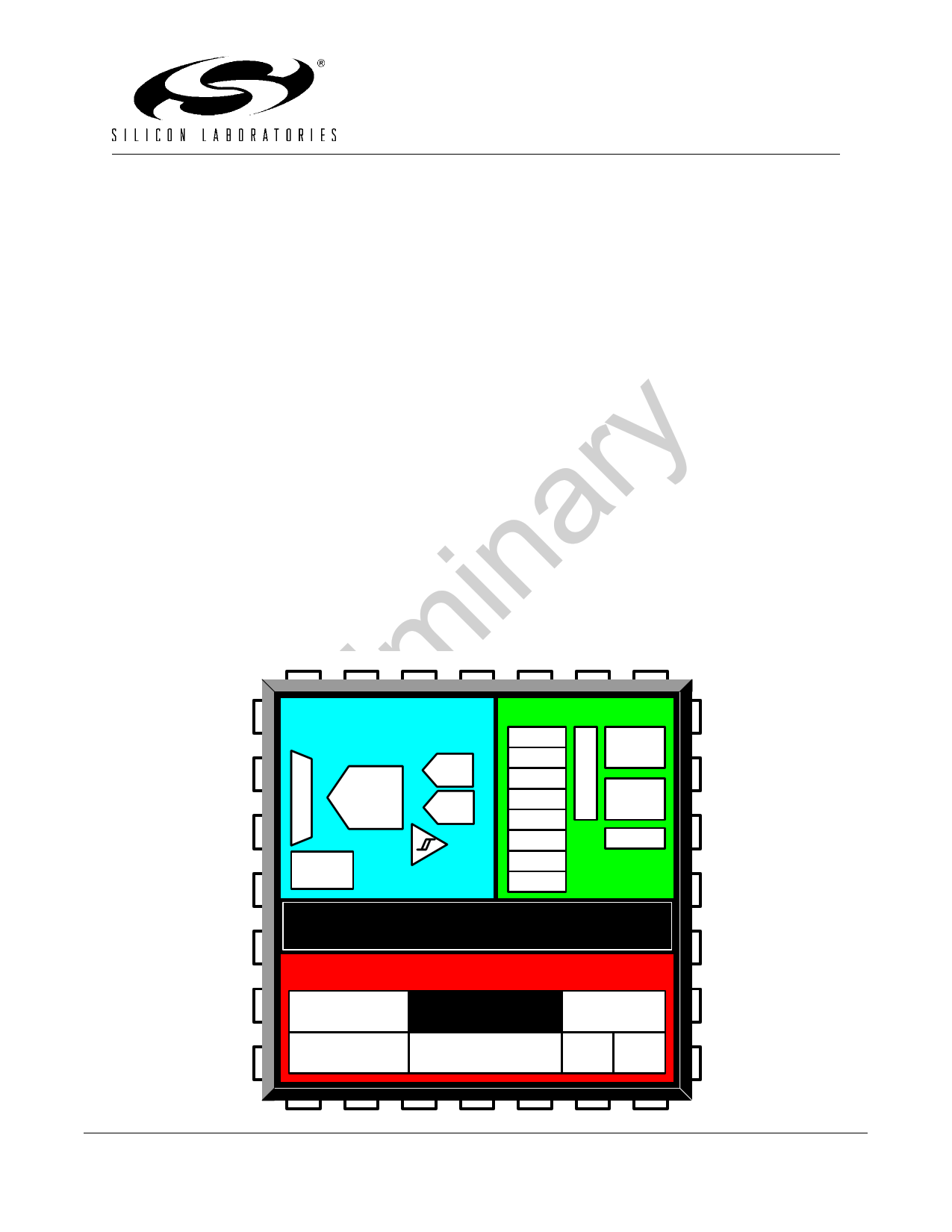
ANALOG
PERIPHERALS
8-bit
A
24-bit
IDAC
M
U
1ksps
8-bit
X
ADC
IDAC
+
TEMP
SENSOR
-
VOLTAGE
COMPARATOR
DIGITAL I/O
UART
SMBus
Port 0
SPI
PCA
Port 1
Timer 0
Timer 1
P2.0
Timer 2
Timer 3
24.5 MHz PRECISION INTERNAL OSCILLATOR
WITH CLOCK MULTIPLIER
HIGH-SPEED CONTROLLER CORE
8KB
ISP FLASH
FLEXIBLE
INTERRUPTS
8051 CPU
(50 MIPS)
DEBUG
CIRCUITRY
768 B SRAM
POR WDT
Preliminary Rev. 0.4 1/04
Copyright © 2004 by Silicon Laboratories
C8051F350/1/2/3-DS04
This information applies to a product under development. Its characteristics and specifications are subject to change without notice.
1 page 
C8051F350/1/2/3
17.2.External Oscillator Drive Circuit...................................................................... 127
17.2.1.Clocking Timers Directly Through the External Oscillator...................... 127
17.2.2.External Crystal Example....................................................................... 127
17.2.3.External RC Example............................................................................. 128
17.2.4.External Capacitor Example................................................................... 128
17.3.Clock Multiplier ............................................................................................... 130
17.4.System Clock Selection.................................................................................. 131
18. Port Input/Output.................................................................................................. 133
18.1.Priority Crossbar Decoder .............................................................................. 135
18.2.Port I/O Initialization ....................................................................................... 137
18.3.General Purpose Port I/O ............................................................................... 140
19. SMBus ................................................................................................................... 147
19.1.Supporting Documents ................................................................................... 148
19.2.SMBus Configuration...................................................................................... 148
19.3.SMBus Operation ........................................................................................... 149
19.3.1.Arbitration............................................................................................... 149
19.3.2.Clock Low Extension.............................................................................. 150
19.3.3.SCL Low Timeout................................................................................... 150
19.3.4.SCL High (SMBus Free) Timeout .......................................................... 150
19.4.Using the SMBus............................................................................................ 151
19.4.1.SMBus Configuration Register............................................................... 152
19.4.2.SMB0CN Control Register ..................................................................... 155
19.4.3.Data Register ......................................................................................... 158
19.5.SMBus Transfer Modes.................................................................................. 159
19.5.1.Master Transmitter Mode ....................................................................... 159
19.5.2.Master Receiver Mode ........................................................................... 160
19.5.3.Slave Receiver Mode ............................................................................. 161
19.5.4.Slave Transmitter Mode ......................................................................... 162
19.6.SMBus Status Decoding................................................................................. 163
20. UART0.................................................................................................................... 167
20.1.Enhanced Baud Rate Generation................................................................... 168
20.2.Operational Modes ......................................................................................... 169
20.2.1.8-Bit UART ............................................................................................. 169
20.2.2.9-Bit UART ............................................................................................. 170
20.3.Multiprocessor Communications .................................................................... 171
21. Serial Peripheral Interface (SPI0) ........................................................................ 177
21.1.Signal Descriptions......................................................................................... 178
21.1.1.Master Out, Slave In (MOSI).................................................................. 178
21.1.2.Master In, Slave Out (MISO).................................................................. 178
21.1.3.Serial Clock (SCK) ................................................................................. 178
21.1.4.Slave Select (NSS) ................................................................................ 178
21.2.SPI0 Master Mode Operation ......................................................................... 179
21.3.SPI0 Slave Mode Operation ........................................................................... 181
21.4.SPI0 Interrupt Sources ................................................................................... 181
21.5.Serial Clock Timing......................................................................................... 182
Rev. 0.4
5
5 Page 
C8051F350/1/2/3
Table 20.6. Timer Settings for Standard Baud Rates Using an External Oscillator 176
21. Serial Peripheral Interface (SPI0) ....................................................................... 177
Figure 21.1. SPI Block Diagram ............................................................................. 177
Figure 21.2. Multiple-Master Mode Connection Diagram ....................................... 180
Figure 21.3. 3-Wire Single Master and Single Slave Mode Connection Diagram .. 180
Figure 21.4. 4-Wire Single Master and Slave Mode Connection Diagram ............. 180
Figure 21.5. Data/Clock Timing Relationship ......................................................... 182
Figure 21.6. SPI0CFG: SPI0 Configuration Register ............................................. 183
Figure 21.7. SPI0CN: SPI0 Control Register.......................................................... 184
Figure 21.8. SPI0CKR: SPI0 Clock Rate Register ................................................. 185
Figure 21.9. SPI0DAT: SPI0 Data Register............................................................ 186
Figure 21.10. SPI Master Timing (CKPHA = 0)...................................................... 187
Figure 21.11. SPI Master Timing (CKPHA = 1)...................................................... 187
Figure 21.12. SPI Slave Timing (CKPHA = 0)........................................................ 188
Figure 21.13. SPI Slave Timing (CKPHA = 1)........................................................ 188
Table 21.1. SPI Slave Timing Parameters ............................................................. 189
22. Timers ................................................................................................................... 191
Figure 22.1. T0 Mode 0 Block Diagram.................................................................. 192
Figure 22.2. T0 Mode 2 Block Diagram.................................................................. 193
Figure 22.3. T0 Mode 3 Block Diagram.................................................................. 194
Figure 22.4. TCON: Timer Control Register ........................................................... 195
Figure 22.5. TMOD: Timer Mode Register ............................................................. 196
Figure 22.6. CKCON: Clock Control Register ........................................................ 197
Figure 22.7. TL0: Timer 0 Low Byte ....................................................................... 198
Figure 22.8. TL1: Timer 1 Low Byte ....................................................................... 198
Figure 22.9. TH0: Timer 0 High Byte...................................................................... 198
Figure 22.10. TH1: Timer 1 High Byte.................................................................... 198
Figure 22.11. Timer 2 16-Bit Mode Block Diagram ................................................ 199
Figure 22.12. Timer 2 8-Bit Mode Block Diagram .................................................. 200
Figure 22.13. TMR2CN: Timer 2 Control Register ................................................. 201
Figure 22.14. TMR2RLL: Timer 2 Reload Register Low Byte ................................ 202
Figure 22.15. TMR2RLH: Timer 2 Reload Register High Byte............................... 202
Figure 22.16. TMR2L: Timer 2 Low Byte................................................................ 202
Figure 22.17. TMR2H Timer 2 High Byte ............................................................... 202
Figure 22.18. Timer 3 16-Bit Mode Block Diagram ................................................ 203
Figure 22.19. Timer 3 8-Bit Mode Block Diagram .................................................. 204
Figure 22.20. TMR3CN: Timer 3 Control Register ................................................. 205
Figure 22.21. TMR3RLL: Timer 3 Reload Register Low Byte ................................ 206
Figure 22.22. TMR3RLH: Timer 3 Reload Register High Byte............................... 206
Figure 22.23. TMR3L: Timer 3 Low Byte................................................................ 206
Figure 22.24. TMR3H Timer 3 High Byte ............................................................... 206
23. Programmable Counter Array ............................................................................ 207
Figure 23.1. PCA Block Diagram............................................................................ 207
Figure 23.2. PCA Counter/Timer Block Diagram.................................................... 208
Table 23.1. PCA Timebase Input Options .............................................................. 208
Rev. 0.4
11
11 Page | ||
| Páginas | Total 30 Páginas | |
| PDF Descargar | [ Datasheet C8051F353.PDF ] | |
Hoja de datos destacado
| Número de pieza | Descripción | Fabricantes |
| C8051F350 | 8k ISP Flash MCU | Silicon Laboratories |
| C8051F351 | 8k ISP Flash MCU | Silicon Laboratories |
| C8051F352 | 8k ISP Flash MCU | Silicon Laboratories |
| C8051F353 | 8k ISP Flash MCU | Silicon Laboratories |
| Número de pieza | Descripción | Fabricantes |
| SLA6805M | High Voltage 3 phase Motor Driver IC. |
Sanken |
| SDC1742 | 12- and 14-Bit Hybrid Synchro / Resolver-to-Digital Converters. |
Analog Devices |
|
DataSheet.es es una pagina web que funciona como un repositorio de manuales o hoja de datos de muchos de los productos más populares, |
| DataSheet.es | 2020 | Privacy Policy | Contacto | Buscar |