|
|
|
PDF CAT25010 Data sheet ( Hoja de datos )
| Número de pieza | CAT25010 | |
| Descripción | 1K/2K/4K SPI Serial CMOS EEPROM | |
| Fabricantes | Catalyst Semiconductor | |
| Logotipo | ||
Hay una vista previa y un enlace de descarga de CAT25010 (archivo pdf) en la parte inferior de esta página. Total 11 Páginas | ||
|
No Preview Available !
CAT25010/20/40
1K/2K/4K SPI Serial CMOS EEPROM
FEATURES
s 10 MHz SPI compatible
s 1.8 to 6.0 volt operation
s Hardware and software protection
s Low power CMOS technology
s SPI modes (0,0 & 1,1)*
s Commercial, industrial, automotive and extended
temperature ranges
ALOGEN FR
LEA D F REETM
s 1,000,000 program/erase cycles
s 100 year data retention
s Self-timed write cycle
s 8-Pin DIP/SOIC, 8-Pin TSSOP and 8-Pin MSOP
s 16-byte page write buffer
s Block write protection
– Protect 1/4, 1/2 or all of EEPROM array
DESCRIPTION
The CAT25010/20/40 is a 1K/2K/4K Bit SPI Serial
CMOS EEPROM internally organized as 128x8/256x8/
512x8 bits. Catalyst’s advanced CMOS Technology
substantially reduces device power requirements. The
CAT25010/20/40 features a 16-byte page write buffer.
The device operates via the SPI bus serial interface and
is enabled though a Chip Select (CS). In addition to the
Chip Select, the clock input (SCK), data in (SI) and data
out (SO) are required to access the device. The HOLD
pin may be used to suspend any serial communication
without resetting the serial sequence. The CAT25010/
20/40 is designed with software and hardware write
protection features including Block Write protection. The
device is available in 8-pin DIP, 8-pin SOIC, 8-pin MSOP
and 8-pin TSSOP packages.
PIN CONFIGURATION
SOIC Package (S, V)
CS 1
SO 2
WP
VSS
3
4
8 VCC
7 HOLD
6 SCK
5 SI
MSOP Package (R, Z)*
CS 1
SO 2
WP 3
VSS 4
8 VCC
7 HOLD
6 SCK
5 SI
*CAT 25010/20 only
DIP Package (P, L)
TSSOP Package (U, Y)
CS
SO
WP
VSS
1
2
3
4
8 VCC
7 HOLD
6 SCK
5 SI
CS
SO
WP
VSS
1
2
3
4
8 VCC
7 HOLD
6 SCK
5 SI
PIN FUNCTIONS
Pin Name
Function
SO Serial Data Output
SCK
Serial Clock
WP Write Protect
VCC +1.8V to +6.0V Power Supply
VSS Ground
CS Chip Select
SI Serial Data Input
HOLD
Suspends Serial Input
NC No Connect
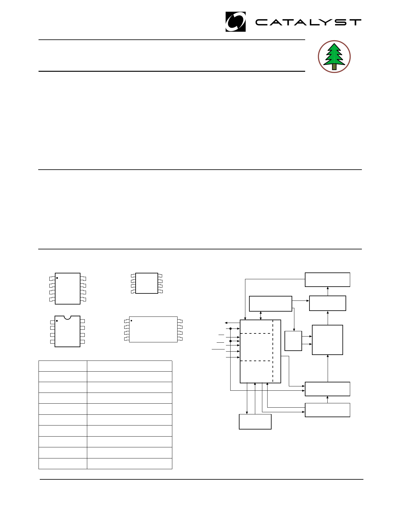
BLOCK DIAGRAM
SENSE AMPS
SHIFT REGISTERS
SO
SI
CS
WP
HOLD
SCK
WORD ADDRESS
BUFFERS
COLUMN
DECODERS
I/O
CONTROL
SPI
CONTROL
LOGIC
BLOCK
PROTECT
LOGIC
STATUS
REGISTER
XDEC
E2PROM
ARRAY
DATA IN
STORAGE
HIGH VOLTAGE/
TIMING CONTROL
25C128 F02
* Other SPI modes available on request.
© 2004 by Catalyst Semiconductor, Inc.
Characteristics subject to change without notice
1
Doc. No. 1006, Rev. L
1 page 
CAT25010/20/40
clock for SPI modes (0,0 & 1,1).
SCK: Serial Clock
SCK is the serial clock pin. This pin is used to synchronize
the communication between the microcontroller and the
CAT25010/20/40. Opcodes, byte addresses, or data
present on the SI pin are latched on the rising edge of the
SCK. Data on the SO pin is updated on the falling edge
of the SCK for SPI modes (0,0 & 1,1) .
CS: Chip Select
CS is the Chip select pin. CS low enables the CAT25010/
20/40 and CS high disables the CAT25010/20/40. CS
high takes the SO output pin to high impedance and
forces the devices into a Standby Mode (unless an
internal write operation is underway) The CAT25010/
20/40 draws ZERO current in the Standby mode. A high
to low transition on CS is required prior to any sequence
being initiated. A low to high transition on CS after a valid
write sequence is what initiates an internal write cycle.
STATUS REGISTER
7654
1111
WP: Write Protect
WP is the Write Protect pin. The Write Protect pin will
allow normal read/write operations when held high.
When WP is tied low all write operations are inhibited.
WP held low while CS is low will interrupt a write to the
CAT25010/20/40. If the internal write cycle has already
been initiated, WP going low will have no effect on any
write operation. Figure 10 illustrates the WP timing
sequence during a write operation.
HOLD: Hold
The HOLD pin is used to pause transmission to the
CAT25010/20/40 while in the middle of a serial sequence
without having to re-transmit entire sequence at a later
time. To pause, HOLD must be brought low while SCK
is low. The SO pin is in a high impedance state during
the time the part is paused, and transitions on the SI pins
will be ignored. To resume communication, HOLD is
brought high, while SCK is low. (HOLD should be held
high any time this function is not being used.) HOLD may
be tied high directly to VCC or tied to VCC through a
resistor. Figure 9 illustrates hold timing sequence.
3210
BP1
BP0
WEL
RDY
BLOCK PROTECTION BITS
Status Register Bits
BP1 BP0
00
01
10
11
Array Address
Protected
None
25010: 60-7F
25020: C0-FF
25040: 180-1FF
25010: 40-7F
25020: 80-FF
25040: 100-1FF
25010: 00-7F
25020: 00-FF
25040: 000-1FF
Protection
No Protection
Quarter Array Protection
Half Array Protection
Full Array Protection
5 Doc. No. 1006, Rev. L
5 Page 
REVISION HISTORY
Date
8/3/2004
Rev.
L
Reason
Updated Features
Updated DC Operating Characteristics table & notes
CAT25010/20/40
Copyrights, Trademarks and Patents
Trademarks and registered trademarks of Catalyst Semiconductor include each of the following:
DPP ™ AE2 ™
Catalyst Semiconductor has been issued U.S. and foreign patents and has patent applications pending that protect its products. For a complete list of patents
issued to Catalyst Semiconductor contact the Company’s corporate office at 408.542.1000.
CATALYST SEMICONDUCTOR MAKES NO WARRANTY, REPRESENTATION OR GUARANTEE, EXPRESS OR IMPLIED, REGARDING THE SUITABILITY OF ITS
PRODUCTS FOR ANY PARTICULAR PURPOSE, NOR THAT THE USE OF ITS PRODUCTS WILL NOT INFRINGE ITS INTELLECTUAL PROPERTY RIGHTS OR THE
RIGHTS OF THIRD PARTIES WITH RESPECT TO ANY PARTICULAR USE OR APPLICATION AND SPECIFICALLY DISCLAIMS ANY AND ALL LIABILITY ARISING
OUT OF ANY SUCH USE OR APPLICATION, INCLUDING BUT NOT LIMITED TO, CONSEQUENTIAL OR INCIDENTAL DAMAGES.
Catalyst Semiconductor products are not designed, intended, or authorized for use as components in systems intended for surgical implant into the body, or
other applications intended to support or sustain life, or for any other application in which the failure of the Catalyst Semiconductor product could create a
situation where personal injury or death may occur.
Catalyst Semiconductor reserves the right to make changes to or discontinue any product or service described herein without notice. Products with data sheets
labeled "Advance Information" or "Preliminary" and other products described herein may not be in production or offered for sale.
Catalyst Semiconductor advises customers to obtain the current version of the relevant product information before placing orders. Circuit diagrams illustrate
typical semiconductor applications and may not be complete.
Catalyst Semiconductor, Inc.
Corporate Headquarters
1250 Borregas Avenue
Sunnyvale, CA 94089
Phone: 408.542.1000
Fax: 408.542.1200
www.catalyst-semiconductor.com
11
Publication #: 1006
Revison:
L
Issue date: 8/3/04
Doc. No. 1006, Rev. L
11 Page | ||
| Páginas | Total 11 Páginas | |
| PDF Descargar | [ Datasheet CAT25010.PDF ] | |
Hoja de datos destacado
| Número de pieza | Descripción | Fabricantes |
| CAT25010 | 1K/2K/4K SPI Serial CMOS EEPROM | Catalyst Semiconductor |
| CAT25010 | (CAT25010 - CAT25040) SPI Serial CMOS EEPROM | ON Semiconductor |
| Número de pieza | Descripción | Fabricantes |
| SLA6805M | High Voltage 3 phase Motor Driver IC. |
Sanken |
| SDC1742 | 12- and 14-Bit Hybrid Synchro / Resolver-to-Digital Converters. |
Analog Devices |
|
DataSheet.es es una pagina web que funciona como un repositorio de manuales o hoja de datos de muchos de los productos más populares, |
| DataSheet.es | 2020 | Privacy Policy | Contacto | Buscar |