|
|
|
PDF 24LC160 Data sheet ( Hoja de datos )
| Número de pieza | 24LC160 | |
| Descripción | Bus Serial EEPROM | |
| Fabricantes | Microchip | |
| Logotipo | ||
Hay una vista previa y un enlace de descarga de 24LC160 (archivo pdf) en la parte inferior de esta página. Total 12 Páginas | ||
|
No Preview Available !
25LC080/160
8K/16K 2.5V SPI™ Bus Serial EEPROM
FEATURES
• SPI modes 0,0 and 1,1
• 3 MHz Clock Rate
• Single supply with programming operation down
to 2.5V
• Low Power CMOS Technology
- Max Write Current: 5 mA
- Read Current: 1.0 mA
- Standby Current: 1 µA typical
• Organization
- 1024 x 8 for 25LC080
- 2048 x 8 for 25LC160
• 16 Byte Page
• Sequential Read
• Self-timed ERASE and WRITE Cycles
• Block Write Protection
- Protect none, 1/4, 1/2, or all of Array
• Built-in Write Protection
- Power On/Off Data Protection Circuitry
- Write Latch
- Write Protect Pin
• High Reliability
- Endurance: 10M cycles (guaranteed)
- Data Retention: >200 years
- ESD protection: >4000 V
• 8-pin PDIP/SOIC Packages
• Temperature ranges supported
- Commercial (C): 0°C to +70°C
- Industrial (I): -40°C to +85°C
DESCRIPTION
The Microchip Technology Inc. 25LC080/160 are 8K
and 16K bit Serial Electrically Erasable PROMs. The
memory is accessed via a simple Serial Peripheral
Interface (SPI) compatible serial bus. The bus signals
required are a clock input (SCK) plus separate data in
(SI) and data out (SO) lines. Access to the device is
controlled through a chip select (CS) input, allowing any
number of devices to share the same bus.
There are two other inputs that provide the end user
with additional flexibility. Communication to the device
can be paused via the hold pin (HOLD). While the
device is paused, transitions on its inputs will be
ignored, with the exception of chip select, allowing the
host to service higher priority interrupts. Also, write
operations to the Status Register can be disabled via
the write protect pin (WP).
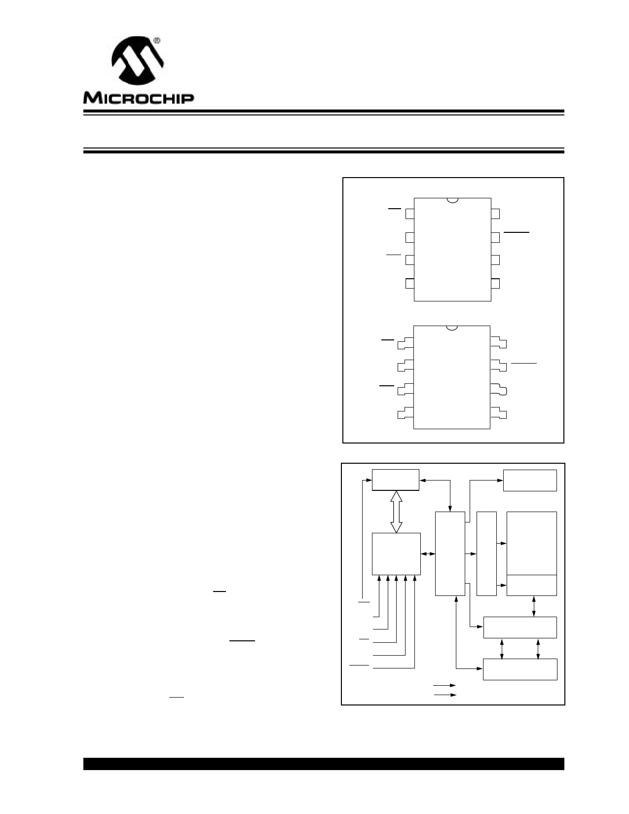
PACKAGE TYPES
PDIP
CS 1
SO 2
WP 3
VSS 4
SOIC
CS
SO
WP
VSS
1
2
3
4
BLOCK DIAGRAM
Status
Register
8 VCC
7 HOLD
6 SCK
5 SI
8 VCC
7 HOLD
6 SCK
5 SI
HV Generator
I/O Control
Logic
Memory
Control
Logic
X
Dec
EEPROM
Array
Page Latches
WP
SI
SO
CS
SCK
HOLD
Vcc
Vss
Y Decoder
Sense Amp.
R/W Control
SPI is a trademark of Motorola.
© 1996 Microchip Technology Inc.
Preliminary
This document was created with FrameMaker 4 0 4
DS21145D-page 1
1 page 
2.0 PRINCIPLES OF OPERATION
The 25LC080/160 is an 1024/2048 byte EEPROM
designed to interface directly with the Serial Peripheral
Interface (SPI) port of many of today’s popular micro-
controller families, including Microchip’s midrange
PIC16CXX microcontrollers. It may also interface with
microcontrollers that do not have a built-in SPI port by
using discrete I/O lines programmed properly with soft-
ware.
The 25LC080/160 contains an 8-bit instruction register.
The part is accessed via the SI pin, with data being
clocked in on the rising edge of SCK. If the WPEN bit in
the status register is set, the WP pin must be held high
to allow writing to the non-volatile bits in the status reg-
ister.
Table 2-1 contains a list of the possible instruction bytes
and format for device operation. All instructions,
addresses and data are transferred MSB first, LSB last.
Data is sampled on the first rising edge of SCK after CS
goes low. If the clock line is shared with other peripheral
devices on the SPI bus, the user can assert the HOLD
input and place the 25LC080/160 in ‘HOLD’ mode.
After releasing the HOLD pin, operation will resume
from the point when the HOLD was asserted.
2.1 Write Enable (WREN) and Write
Disable (WRDI)
The 25LC080/160 contains a write enable latch. This
latch must be set before any write operation will be
completed internally. The WREN instruction will set the
latch, and the WRDI will reset the latch. The following is
a list of conditions under which the write enable latch
will be reset:
• Power-up
• WRDI instruction successfully executed
• WRSR instruction successfully executed
• WRITE instruction successfully executed
2.2 Read Status Register (RDSR)
The RDSR instruction provides access to the status
register. The status register may be read at any time,
even during a write cycle. The status register is format-
ted as follows:
7 654 3 2 1 0
WPEN X X X BP1 BP0 WEL WIP
The Write-In-Process (WIP) bit indicates whether the
25LC080/160 is busy with a write operation. When set
to a ‘1’ a write is in progress, when set to a ‘0’ no write
is in progress. This bit is read only.
The Write Enable Latch (WEL) bit indicates the status
of the write enable latch. When set to a ‘1’ the latch
allows writes to the array and status register, when set
to a ‘0’ the latch prohibits writes to the array and status
register. The state of this bit can always be updated via
25LC080/160
the WREN or WRDI commands regardless of the state
of write protection on the status register. This bit is read
only.
The Block Protection (BP0 and BP1) bits indicate
which blocks are currently write protected. These bits
are set by the user issuing the WRSR instruction.
These bits are non-volatile.
The Write Protect Enable (WPEN) bit is a non-volatile
bit that is available as an enable bit for the WP pin. The
Write Protect (WP) pin and the Write Protect Enable
(WPEN) bit in the status register control the program-
mable hardware write protect feature. Hardware write
protection is enabled when WP pin is low and the
WPEN bit is high. Hardware write protection is disabled
when either the WP pin is high or the WPEN bit is low.
When the chip is hardware write protected, only writes
to non-volatile bits in the status register are disabled.
See Table 2-2 for matrix of functionality on the WPEN
bit and Figure 2-1 for a flowchart of Table 2-2.
See Figure 3-5 for RDSR timing sequence.
TABLE 2-1: INSTRUCTION SET
Instruction Instruction
Name
Format
Description
WREN
WRDI
RDSR
WRSR
READ
WRITE
0000 0110
Set the write enable
latch (enable write
operations)
0000 0100
Reset the write
enable latch (disable
write operations)
0000 0101 Read status register
0000 0001
Write status register
(write protect enable
and block write pro-
tection bits)
0000 0011
Read data from
memory array begin-
ning at selected
address
0000 0010
Write data to memory
array beginning at
selected address
© 1996 Microchip Technology Inc.
Preliminary
DS21145D-page 5
5 Page 
25LC080/160
25LC080/160 Product Identification System
To order or to obtain information (e.g., on pricing or delivery), please use the listed part numbers, and refer to the factory or the listed
sales offices.
25LC080/160 -
/P
Package:
P = Plastic DIP (300 mil body), 8 lead
SN = Plastic SOIC (150 mil body), 8 lead
Temperature
Range:
Blank = 0°C to +70°C
I = -40°C to +85°C
Device:
25LC080/160
25LC080T/160T
SPI Bus Serial EEPROM
SPI Bus Serial EEPROM (Tape and Reel)
Sales and Support
Products supported by a preliminary Data Sheet may possibly have an errata sheet describing minor operational differences and
recommended workarounds. To determine if an errata sheet exists for a particular device, please contact one of the following:
1. Your local Microchip sales office (see next page)
2. The Microchip Corporate Literature Center U.S. FAX: (602) 786-7277
3. The Microchip’s Bulletin Board, via your local CompuServe number (CompuServe membership NOT required).
Please specify which device, revision of silicon and Data Sheet (include Literature #) you are using.
For latest version information and upgrade kits for Microchip Development Tools, please call 1-800-755-2345 or 1-602-786-7302.
© 1996 Microchip Technology Inc.
Preliminary
DS21145D-page 11
11 Page | ||
| Páginas | Total 12 Páginas | |
| PDF Descargar | [ Datasheet 24LC160.PDF ] | |
Hoja de datos destacado
| Número de pieza | Descripción | Fabricantes |
| 24LC160 | Bus Serial EEPROM | Microchip |
| 24LC16B | EEPROM | MicrochipTechnology |
| Número de pieza | Descripción | Fabricantes |
| SLA6805M | High Voltage 3 phase Motor Driver IC. |
Sanken |
| SDC1742 | 12- and 14-Bit Hybrid Synchro / Resolver-to-Digital Converters. |
Analog Devices |
|
DataSheet.es es una pagina web que funciona como un repositorio de manuales o hoja de datos de muchos de los productos más populares, |
| DataSheet.es | 2020 | Privacy Policy | Contacto | Buscar |