|
|
|
PDF THC63LVD823B Data sheet ( Hoja de datos )
| Número de pieza | THC63LVD823B | |
| Descripción | 160MHz 51Bits LVDS Transmitter | |
| Fabricantes | THine Electronics | |
| Logotipo | ||
Hay una vista previa y un enlace de descarga de THC63LVD823B (archivo pdf) en la parte inferior de esta página. Total 21 Páginas | ||
|
No Preview Available !
THC63LVD823B_Rev.3.1_E
THC63LVD823B
160MHz 51Bits LVDS Transmitter
General Description
The THC63LVD823B transmitter is designed to sup-
port Single Link transmission between Host and Flat
Panel Display and Dual Link transmission between
Host and Flat Panel Display up to 1080p/QXGA resolu-
tions.
The THC63LVD823B converts 51bits of CMOS/TTL
data into LVDS (Low Voltage Differential Signaling)
data stream. The transmitter can be programmed for ris-
ing edge or falling edge clocks through a dedicated pin.
In Dual Link, the transmit clock frequency of 160MHz,
51bits of RGB data are transmitted at an effective rate
of 1.12Gbps per LVDS channel.
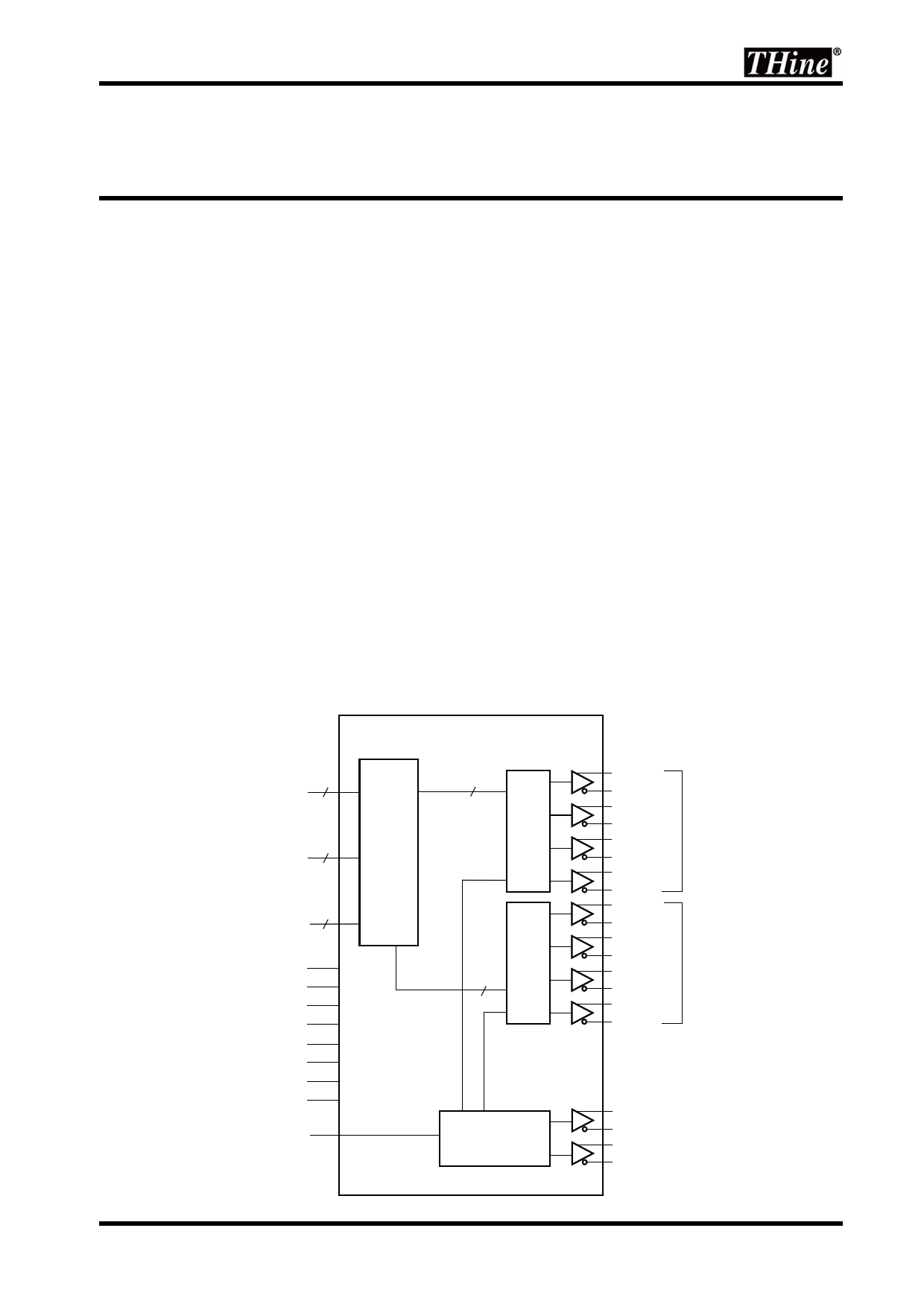
Block Diagram
Features
• Wide dot clock range suited for TV Signal (480p-
1080p), PC Signal (VGA-QXGA)
TTL/CMOS Input: 10-160MHz
LVDS Output: 20-160MHz
• PLL requires No external components
• Flexible Input/Output mode
1. Single/Dual TTL IN, Single/Dual LVDS OUT
2. Double edge input for Single TTL IN/Dual LVDS OUT
• Clock edge selectable
• 2 LVDS data mapping for simplifying PCB layout.
• Pseudo Random pattern generation circuit
• Supports Reduced swing LVDS for Low EMI
• Power down mode
• Low power single 3.3V CMOS design
• 1.2 up to 3.3V tolerant data inputs to connect
directly to low power,low voltage application and
graphic processor.
• Backward compatible with THC63LVD823/
THC63LVD823A
• 100pin TQFP
DATA Port1
R1[7:0]
G1[7:0]
B1[7:0]
24
DATA Port2
R2[7:0]
G2[7:0]
B2[7:0]
24
HSYNC
VSYNC
DE
3
R/F
RS
MAP
MODE[1:0]
O/E
DDRN
/PDWN
PRBS
TRANSMITTER CLOCK IN
(10 to 160MHz)
Copyright©2011 THine Electronics, Inc.
28
28
TA1 +/-
TB1 +/-
TC1 +/-
TD1 +/-
TA2 +/-
TB2 +/-
TC2 +/-
TD2 +/-
LVDS OUTPUT
Port1
LVDS OUTPUT
Port2
TCLK1 +/-
PLL
TCLK2 +/- (N/C)
(20 to 160MHz)
1/21 THine Electronics, Inc.
1 page 
THC63LVD823B_Rev.3.1_E
Absolute Maximum Ratings
Supply Voltage (VCC)
CMOS/TTL Input Voltage
LVDS Transmitter Output Voltage
Output Current
Junction Temperature
Storage Temperature Range
Reflow Peak Temperature / Time
Maximum Power Dissipation @+25 °C
Recommended Operating Conditions
-0.3V ~ +4.0V
-0.3V ~ (VCC + 0.3V)
-0.3V ~ (VCC + 0.3V)
-30mA ~ 30mA
+125 ° C
-55°C ~ +125°C
+260°C / 10sec.
2.4W
Clock
Frequency
Parameter
All Supply Voltage
Operating Ambient Temperature
MODE<1:0>=LL
Dual-in/Dual-out
MODE<1:0>=LH
Dual-in/Single-out
Single Edge Input
MODE<1:0>=HL (DDRN =Open/H)
Single-in/Dual-out Double Edge Input
(DDRN=L)
MODE<1:0>=HH
Single-in/Single-out
Input
LVDS Output
Input
LVDS Output
Input
LVDS Output
Input
LVDS Output
Input
LVDS Output
Min. Typ Max Units
3.0 3.3 3.6 V
-20 70 °C
20 160 MHz
20 160 MHz
10 80 MHz
20 160 MHz
40 160 MHz
20 80 MHz
20 80 MHz
20 80 MHz
20 160 MHz
20 160 MHz
Copyright©2011 THine Electronics, Inc.
5/21 THine Electronics, Inc.
5 Page 
THC63LVD823B_Rev.3.1_E
AC Timing Diagrams (Continued)
tTOP2
tTOP3
tTOP4
tTOP5
tTOP6
tTOP0
tTOP1
Tyx+/-
Tyx6 Tyx5 Tyx4 Tyx3 Tyx2 Tyx1 Tyx0 Tyx6 Tyx5 Tyx4 Tyx3 Tyx2 Tyx1
TCLKx+
x = 1,2
y = A,B,C,D
Vdiff = 0V
Vdiff = 0V
tTCOP
Note:
Vdiff = (Tyx+) - (Tyx-), (TCLKx+) - (TCLKx-)
Fig6. LVDS Output Data Position
Copyright©2011 THine Electronics, Inc.
11/21
THine Electronics, Inc.
11 Page | ||
| Páginas | Total 21 Páginas | |
| PDF Descargar | [ Datasheet THC63LVD823B.PDF ] | |
Hoja de datos destacado
| Número de pieza | Descripción | Fabricantes |
| THC63LVD823 | LVDS Transmitter | THine Electronics |
| THC63LVD823B | 160MHz 51Bits LVDS Transmitter | THine Electronics |
| Número de pieza | Descripción | Fabricantes |
| SLA6805M | High Voltage 3 phase Motor Driver IC. |
Sanken |
| SDC1742 | 12- and 14-Bit Hybrid Synchro / Resolver-to-Digital Converters. |
Analog Devices |
|
DataSheet.es es una pagina web que funciona como un repositorio de manuales o hoja de datos de muchos de los productos más populares, |
| DataSheet.es | 2020 | Privacy Policy | Contacto | Buscar |