|
|
|
PDF HMC856 Data sheet ( Hoja de datos )
| Número de pieza | HMC856 | |
| Descripción | Digital Time Delay | |
| Fabricantes | Analog Devices | |
| Logotipo | ||
Hay una vista previa y un enlace de descarga de HMC856 (archivo pdf) en la parte inferior de esta página. Total 14 Páginas | ||
|
No Preview Available !
Data Sheet
28 Gbps, 5-Bit, Digital Time Delay with
Programmable Output Voltage
HMC856
FEATURES
Differential and single-ended operation
Supports data rates up to 28 Gbps
Fast rise/fall time: 20 ps/18 ps
Low power consumption: 610 mW typical
Programmable differential
Output voltage swing: 500 mV p-p to 1350 mV p-p
Single supply: −3.3 V
5 mm × 5 mm, 32-terminal ceramic leadless chip carrier (LCC)
package: 25 mm2
APPLICATIONS
SONET OC-192
High speed serial logic
Clock and data recovery
Broadband test and measurement equipment
Frequency synthesis
Matched timing
GENERAL DESCRIPTION
The HMC856 is a wideband time delay device with a 5-bit
digital control designed for timing compensation or clock skew
management applications. The time delay provides nearly
100 ps (maximum) of delay range with 3 ps resolution and
supports 28 Gbps data. The monotonic delay is compensated
for stable operation over both power supply and temperature
variation.
All differential inputs to the HMC856 are current mode logic
(CML) and terminated on chip with 50 Ω to the positive supply
ground, GND, and can be ac or dc-coupled. The differential CML
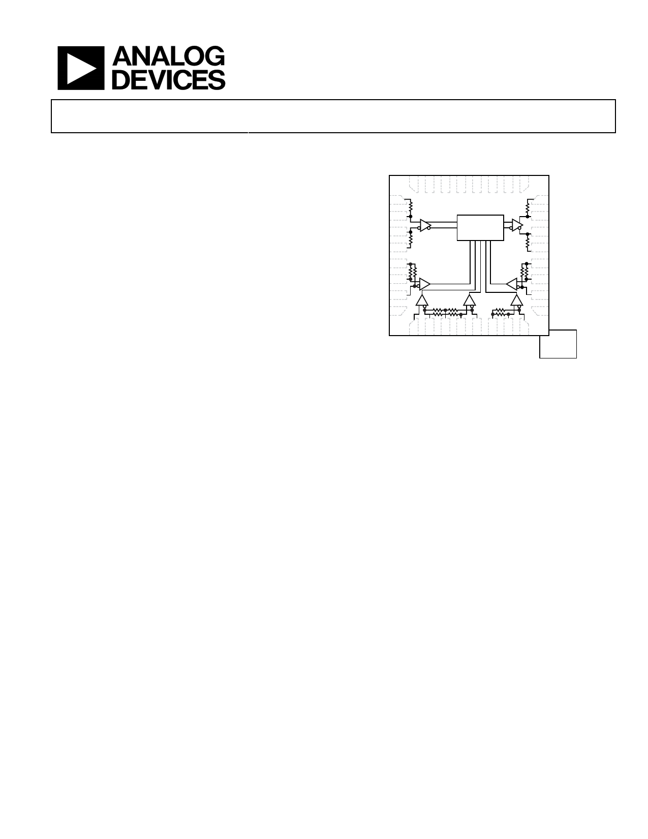
FUNCTIONAL BLOCK DIAGRAM
GND 1
I+ 2
I– 3
GND 4
GND 5
B0+ 6
B0– 7
NC 8
50Ω HMC856 50Ω
DELAY
50Ω 50Ω
600Ω
600Ω
600Ω 600Ω
600Ω
24 GND
23 O+
22 O–
21 GND
20 GND
19 B4+
18 B4–
17 NC
Figure 1.
PACKAGE
BASE
VEE
outputs are source terminated to 50 Ω and can also be ac or dc-
coupled. Connect outputs directly to a 50 Ω ground terminated
system or drive devices with CML logic input. The control lines,
B4 to B0, are differential CML inputs terminated with 600 Ω to
the positive rail, which supports lower power control options.
The HMC856 features an output level control pin, VR, that
allows loss compensation or signal level optimization. The
HMC856 operates from a single −3.3 V supply and is available
in a 5 mm × 5 mm LCC package.
Rev. C
Document Feedback
Information furnished by Analog Devices is believed to be accurate and reliable. However, no
responsibilityisassumedbyAnalogDevices for itsuse,nor foranyinfringementsofpatentsor other
rights of third parties that may result from its use. Specifications subject to change without notice. No
license is granted by implication or otherwise under any patent or patent rights of Analog Devices.
Trademarksandregisteredtrademarksarethepropertyoftheirrespectiveowners.
One Technology Way, P.O. Box 9106, Norwood, MA 02062-9106, U.S.A.
Tel: 781.329.4700
©2016 Analog Devices, Inc. All rights reserved.
Technical Support
www.analog.com
1 page 
HMC856
ABSOLUTE MAXIMUM RATINGS
Table 2.
Parameter
Power Supply Voltage (VEE)
Input Signals
Output Signals
Maximum Junction Temperature
Continuous Power Dissipation, PDISS
(T = 85°C, Derate 33 mW/°C Above 85°C)
Thermal Resistance, θJC (Worst Case Device
to Package Exposed Paddle)
Temperature
Storage
Operating
Reflow (MSL3 Rating)
ESD Sensitivity Human Body Model (HBM)
Rating
−3.75 V to +0.5 V
−2 V to +0.5 V
−1.5 V to 0.5 V
125°C
1.33 W
30°C/W
−65°C to +150°C
−40°C to +85°C
260°C
Class 1C
Data Sheet
Stresses at or above those listed under Absolute Maximum
Ratings may cause permanent damage to the product. This is a
stress rating only; functional operation of the product at these
or any other conditions above those indicated in the operational
section of this specification is not implied. Operation beyond
the maximum operating conditions for extended periods may
affect product reliability.
ESD CAUTION
Rev. C | Page 4 of 13
5 Page 
HMC856
THEORY OF OPERATION
The HMC856 is a wideband time delay device with a 5-bit digital
control designed for timing compensation or clock skew
management applications. The HMC856 operates from a single
−3.3 V supply and is available in a 5 mm × 5 mm LCC package.
The HMC856 can support data rates up to 28 Gbps and is able
to provide 100 ps variable delay with 3 ps resolution. The total
propagation delay of the HMC856 varies between 250 ps and
350 ps. The maximum achievable delay and bandwidth of the
HMC856 depends on the power of the input signal. If the input
signal is large, the maximum achievable delay is reduced, but the
bandwidth is increased, and because the input signal becomes
smaller, maximum achievable delay is increased and bandwidth is
narrowed.
The HMC856 uses a CML interface, which uses 50 Ω internal
terminations to the ground. The input and output pins can be
interfaced with either ac or dc coupling. For ac coupling, using a
Data Sheet
series resistor, which is effectively short circuit, and an ac load of
50 Ω is recommended. For dc coupling, inputs and outputs can be
directly interfaced with another CML circuit. The control lines, B4
to B0, are also CML, but they are terminated with 600 Ω to the
positive rail for low power operation.
The HMC856 features an output level control pin, VR, that
allows loss compensation or signal level optimization. VR can
have a voltage value between −1.2 V and 0.4 V, which results in
a differential output swing of 500 mV p-p and 1350 mV p-p.
Increasing the output swing affects the rise and fall times. As
VR becomes higher, the rise and fall times increase. Changing
the VR pin also changes the power dissipation because the
HMC856 can consume between 140 mA and 200 mA at room
temperature depending on the VR pin.
Rev. C | Page 10 of 13
11 Page | ||
| Páginas | Total 14 Páginas | |
| PDF Descargar | [ Datasheet HMC856.PDF ] | |
Hoja de datos destacado
| Número de pieza | Descripción | Fabricantes |
| HMC850LC3C | 1:2 FANOUT BUFFER | Hittite Microwave Corporation |
| HMC851LC3C | XOR / XNOR GATE | Hittite Microwave |
| HMC853LC3C | 28 Gbps D-Type Flip-Flop W/Programmable Output Voltage | Hittite Microwave |
| HMC854LC5 | 28 Gbps 4:1 Mux W/Programmable Output Voltage | Hittite Microwave |
| Número de pieza | Descripción | Fabricantes |
| SLA6805M | High Voltage 3 phase Motor Driver IC. |
Sanken |
| SDC1742 | 12- and 14-Bit Hybrid Synchro / Resolver-to-Digital Converters. |
Analog Devices |
|
DataSheet.es es una pagina web que funciona como un repositorio de manuales o hoja de datos de muchos de los productos más populares, |
| DataSheet.es | 2020 | Privacy Policy | Contacto | Buscar |