|
|
|
PDF ADL5354 Data sheet ( Hoja de datos )
| Número de pieza | ADL5354 | |
| Descripción | 2200 MHz to 2700 MHz Dual-Balanced Mixer | |
| Fabricantes | Analog Devices | |
| Logotipo | ||
Hay una vista previa y un enlace de descarga de ADL5354 (archivo pdf) en la parte inferior de esta página. Total 25 Páginas | ||
|
No Preview Available !
Data Sheet
2200 MHz to 2700 MHz, Dual-Balanced
Mixer, LO Buffer, IF Amplifier, and RF Balun
ADL5354
FEATURES
RF frequency range of 2200 MHz to 2700 MHz
IF frequency range of 30 MHz to 450 MHz
Power conversion gain: 8.6 dB
SSB noise figure of 10.6 dB
Input IP3 of 26.1 dBm
Input P1dB of 10.6 dBm
Typical LO power of 0 dBm
Single-ended, 50 Ω RF and LO input ports
High isolation SPDT LO input switch
Single-supply operation: 3.3 V to 5 V
Exposed paddle, 6 mm × 6 mm, 36-lead LFCSP
1500 V HBM/500 V FICDM ESD performance
APPLICATIONS
Cellular base station receivers
Transmit observation receivers
Radio link downconverters
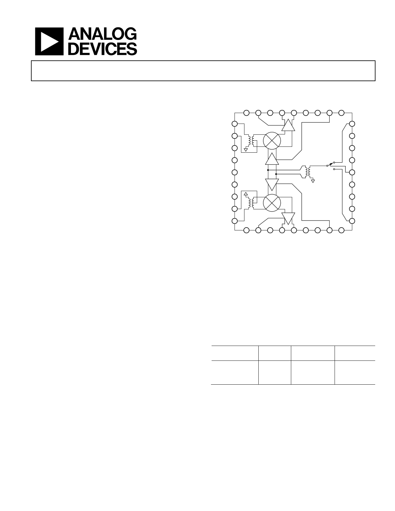
FUNCTIONAL BLOCK DIAGRAM
MNIN 1
MNCT 2
COMM 3
VPOS 4
COMM 5
VPOS 6
COMM 7
DVCT 8
DVIN 9
ADL5354
27 LOI2
26 VGS2
25 VGS1
24 VGS0
23 LOSW
22 PWDN
21 VPOS
20 COMM
19 LOI1
GENERAL DESCRIPTION
The ADL5354 uses a highly linear, doubly balanced, passive mixer
core along with integrated RF and local oscillator (LO) balancing
circuitry to allow single-ended operation. The ADL5354 incor-
porates the RF baluns, allowing for optimal performance over a
2200 MHz to 2700 MHz RF input frequency range. The balanced
passive mixer arrangement provides good LO-to-RF leakage,
typically better than −37 dBm, and excellent intermodulation
performance. The balanced mixer core also provides extremely
high input linearity, allowing the device to be used in demanding
cellular applications where in-band blocking signals may other-
wise result in the degradation of dynamic performance. A high
linearity IF buffer amplifier follows the passive mixer core to yield
a typical power conversion gain of 8 dB and can be used with a
wide range of output impedances.
The ADL5354 provides two switched LO paths that can be used
in time division duplex (TDD) applications where it is desirable
to ping-pong between two local oscillators. LO current can be
externally set using a resistor to minimize dc current
Figure 1.
commensurate with the desired level of performance. For low
voltage applications, the ADL5354 is capable of operation at
voltages as low as 3.3 V with substantially reduced current. For
low voltage operation, an additional logic pin is provided to
power down (approximately 300 µA) the circuit when desired.
The ADL5354 is fabricated using a BiCMOS high performance
IC process. The device is available in a 6 mm × 6 mm, 36-lead
LFCSP and operates over a −40°C to +85°C temperature range.
An evaluation board is also available.
Table 1. Passive Mixers
RF Frequency
(MHz)
Single
Mixer
500 to 1700
ADL5367
1200 to 2500
ADL5365
2200 to 2700
Single Mixer
and IF Amp
ADL5357
ADL5355
ADL5353
Dual Mixer
and IF Amp
ADL5358
ADL5356
ADL5354
Rev. A
Document Feedback
Information furnished by Analog Devices is believed to be accurate and reliable. However, no
responsibility is assumed by Analog Devices for its use, nor for any infringements of patents or other
rights of third parties that may result from its use. Specifications subject to change without notice. No
license is granted by implication or otherwise under any patent or patent rights of Analog Devices.
Trademarksandregisteredtrademarksarethepropertyoftheirrespectiveowners.
One Technology Way, P.O. Box 9106, Norwood, MA 02062-9106, U.S.A.
Tel: 781.329.4700 ©2011–2016 Analog Devices, Inc. All rights reserved.
Technical Support
www.analog.com
1 page 
ADL5354
Data Sheet
5 V PERFORMANCE
VS = 5 V, IS = 350 mA, TA = 25°C, fRF = 2535 MHz, fLO = 2332 MHz, LO power = 0 dBm, RF power = −10 dBm, R1 = R4 = 1.3 kΩ, R2 = R5 = 1 kΩ,
VGS0 = VGS1 = VGS2 = 0 V, and ZO = 50 Ω, unless otherwise noted.
Table 3.
Parameter
DYNAMIC PERFORMANCE
Power Conversion Gain
Voltage Conversion Gain
SSB Noise Figure
Input Third-Order Intercept (IIP3)
Input Second-Order Intercept (IIP2)
Input 1 dB Compression Point (IP1dB)
LO-to-IF Leakage
LO-to-RF Leakage
RF-to-IF Isolation
IF/2 Spurious
IF/3 Spurious
IF Channel-to-Channel Isolation
POWER SUPPLY
Positive Supply Voltage
Quiescent Current
Total Quiescent Current
Test Conditions/Comments
Including 4:1 IF port transformer and PCB loss
ZSOURCE = 50 Ω, differential ZLOAD = 200 Ω differential
fRF1 = 2534.5 MHz, fRF2 = 2535.5 MHz, fLO = 2332 MHz,
each RF tone at −10 dBm
fRF1 = 2535 MHz, fRF2 = 2585 MHz, fLO = 2332 MHz,
each RF tone at −10 dBm
Unfiltered IF output
−10 dBm input power
−10 dBm input power
LO supply
IF supply
VS = 5 V
Min Typ Max Unit
8.6
14.6
10.6
26.1
50
10.6
−20.7
−37
−34
−73
−71
52
dB
dB
dB
dBm
dBm
dBm
dBm
dBm
dBc
dBc
dBc
dB
4.75 5
170
180
350
5.25 V
mA
mA
mA
3.3 V PERFORMANCE
VS = 3.3 V, IS = 200 mA, TA = 25°C, fRF = 2535 MHz, fLO = 2332 MHz, LO power = 0 dBm, R9 = 226 Ω, R14 = 604 Ω, VGS0 = VGS1 = 0 V,
and ZO = 50 Ω, unless otherwise noted.
Table 4.
Parameter
DYNAMIC PERFORMANCE
Power Conversion Gain
Voltage Conversion Gain
SSB Noise Figure
Input Third-Order Intercept (IIP3)
Input Second-Order Intercept (IIP2)
Input 1 dB Compression Point (IP1dB)
POWER INTERFACE
Supply Voltage
Quiescent Current
Power-Down Current
Test Conditions/Comments
Min Typ Max Unit
Including 4:1 IF port transformer and PCB loss
ZSOURCE = 50 Ω, differential ZLOAD = 200 Ω differential
fRF1 = 2534.5 MHz, fRF2 = 2535.5 MHz, fLO = 2332 MHz, each
RF tone at −10 dBm
fRF1 = 2535 MHz, fRF2 = 2585 MHz, fLO = 2332 MHz, each RF
tone at −10 dBm
8
14
9.9
17.5
49
7
dB
dB
dB
dBm
dBm
dBm
Resistor programmable
Device disabled
3.0 3.3 3.6
200
300
V
mA
μA
Rev. A | Page 4 of 24
5 Page 
ADL5354
Data Sheet
VS = 5 V, IS = 350 mA, TA = 25°C, fRF = 2535 MHz, fLO = 2332 MHz, LO power = 0 dBm, RF power = −10 dBm, R1 = R4 = 1.3 kΩ, R2 = R5 = 1 kΩ,
ZO = 50 Ω, VGS0 = VGS1 = VGS2 = 0 V, unless otherwise noted.
12 12.0
11
10
TA = –40°C
9
TA = +25°C
8
TA = +85°C
7
6
11.6
11.2
10.8 TA = +85°C
10.4
TA = +25°C
10.0
9.6
TA = –40°C
9.2
8.8
8.4
5
–6 –4 –2
0
2
4
6
LO POWER (dBm)
8
Figure 21. Power Conversion Gain vs. LO Power
10
8.0
–6 –4 –2
0
2
4
6
LO POWER (dBm)
8 10
Figure 24. Input P1dB vs. LO Power
32
30
28
26
24
22
20
18
16
–6
TA = –40°C
TA = +25°C
TA = +85°C
–4 –2
0
2
4
6
LO POWER (dBm)
Figure 22. Input IP3 vs. LO Power
8 10
–66
–68 TA = –40°C
–70
–72 TA = +85°C
–74
–76 TA = +25°C
–78
–80
2.20 2.25 2.30 2.35 2.40 2.45 2.50 2.55 2.60 2.65 2.70
RF FREQUENCY (GHz)
Figure 25. IF/2 Spurious vs. RF Frequency, RF Power = −10 dBm
58
56
54
52
50
48
46
44
42
40
–6
TA = –40°C
TA = +85°C
TA = +25°C
–4 –2
0
2
4
6
LO POWER (dBm)
Figure 23. Input IP2 vs. LO Power
8
10
–60
–62
–64
–66
TA = +85°C
–68
–70
–72 TA = +25°C
TA = –40°C
–74
2.20 2.25 2.30 2.35 2.40 2.45 2.50 2.55 2.60 2.65 2.70
RF FREQUENCY (GHz)
Figure 26. IF/3 Spurious vs. RF Frequency, RF Power = −10 dBm
Rev. A | Page 10 of 24
11 Page | ||
| Páginas | Total 25 Páginas | |
| PDF Descargar | [ Datasheet ADL5354.PDF ] | |
Hoja de datos destacado
| Número de pieza | Descripción | Fabricantes |
| ADL5350 | LF to 4 GHz High Linearity Y-Mixer | Analog Devices |
| ADL5353 | 2200 MHz to 2700 MHz Balanced Mixer | Analog Devices |
| ADL5354 | 2200 MHz to 2700 MHz Dual-Balanced Mixer | Analog Devices |
| ADL5355 | 1200 MHz to 2500 MHz Balanced Mixer | Analog Devices |
| Número de pieza | Descripción | Fabricantes |
| SLA6805M | High Voltage 3 phase Motor Driver IC. |
Sanken |
| SDC1742 | 12- and 14-Bit Hybrid Synchro / Resolver-to-Digital Converters. |
Analog Devices |
|
DataSheet.es es una pagina web que funciona como un repositorio de manuales o hoja de datos de muchos de los productos más populares, |
| DataSheet.es | 2020 | Privacy Policy | Contacto | Buscar |