|
|
|
PDF ADRF5040 Data sheet ( Hoja de datos )
| Número de pieza | ADRF5040 | |
| Descripción | Nonreflective Switch | |
| Fabricantes | Analog Devices | |
| Logotipo | ||
Hay una vista previa y un enlace de descarga de ADRF5040 (archivo pdf) en la parte inferior de esta página. Total 15 Páginas | ||
|
No Preview Available !
Data Sheet
High Isolation, Silicon SP4T,
Nonreflective Switch, 9 kHz to 12.0 GHz
ADRF5040
FEATURES
Nonreflective 50 Ω design
Positive control range: 0 V to 3.3 V
Low insertion loss: 0.8 dB at 8.0 GHz
High isolation: 34 dB at 8.0 GHz
High power handling
33 dBm through path
27 dBm termination path
High linearity
1 dB compression (P1dB): 37 dBm typical
Input third-order intercept (IIP3): 58 dBm typical at 8.0 GHz
ESD rating: 4 kV human body model (HBM)
4 mm × 4 mm, 24-lead LFCSP package
No low frequency spurious
RF settling time (0.05 dB margin of final RFOUT): 9 µs
APPLICATIONS
Test instrumentation
Microwave radios and very small aperture terminals (VSATs)
Military radios, radars, and electronic counter measures (ECMs)
Fiber optics and broadband telecommunications
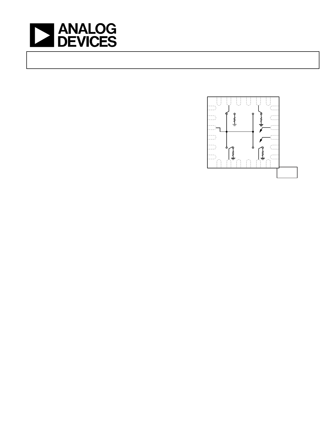
FUNCTIONAL BLOCK DIAGRAM
GND 1
GND 2
RFC 3
GND 4
GND 5
GND 6
ADRF5040
50Ω
50Ω
50Ω 50Ω
18 GND
17 VDD
16 V1
15 V2
14 VSS
13 GND
Figure 1.
PACKAGE
BASE
GND
GENERAL DESCRIPTION
The ADRF5040 is a general-purpose, broadband high isolation,
nonreflective single-pole, quad-throw (SP4T) switch in an LFCSP
surface-mount package. Covering the 9 kHz to 12.0 GHz range,
the switch offers high isolation and low insertion loss. The
switch features 34 dB isolation and 0.8 dB insertion loss up to
8.0 GHz, and a 9 µs settling time of 0.05 dB margin of the final
radio frequency output (RFOUT). The switch operates using
positive control voltage of 3.3 V and 0 V and requires +3.3 V and
−3.3 V supplies. The ADRF5040 is packaged in a 4 mm × 4 mm,
surface-mount LFCSP package.
Rev. A
Document Feedback
Information furnished by Analog Devices is believed to be accurate and reliable. However, no
responsibilityisassumedbyAnalogDevices for itsuse,nor foranyinfringementsofpatentsor other
rights of third parties that may result from its use. Specifications subject to change without notice. No
license is granted by implication or otherwise under any patent or patent rights of Analog Devices.
Trademarksandregisteredtrademarksarethepropertyoftheirrespectiveowners.
One Technology Way, P.O. Box 9106, Norwood, MA 02062-9106, U.S.A.
Tel: 781.329.4700 ©2016–2017 Analog Devices, Inc. All rights reserved.
Technical Support
www.analog.com
1 page 
ADRF5040
Data Sheet
DIGITAL CONTROL VOLTAGE SPECIFICATIONS
VDD = 3.3 V ± 10%, VSS = −3.3 V ± 10%, TCASE = −40°C to +85°C, unless otherwise noted.
Table 2.
Parameter
INPUT CONTROL VOLTAGE (V1, V2)
Low
High
Symbol
VIL
VIH
Min Typ Max
0 0.8
1.4 VDD + 0.3
Unit Test Condition/Comments
<1 µA typical
V
V
BIAS AND SUPPLY CURRENT SPECIFICATIONS
TCASE = −40°C to +85°C, unless otherwise noted.
Table 3.
Parameter
SUPPLY CURRENT
VDD = 3.3 V
VSS = −3.3 V
Symbol
IDD
ISS
Min
Typ
20
20
Max Unit
100 µA
100 µA
Rev. A | Page 4 of 14
5 Page 
ADRF5040
Data Sheet
INPUT POWER COMPRESSION AND INPUT THIRD-ORDER INTERCEPT
VDD = 3.3 V, VSS = −3.3 V, TCASE = 25°C, unless otherwise specified.
44 44
42 42
40 40
38 38
36 36
34 34
32
30 +85°C
+25°C
28 –40°C
32 3.6V
3.3V
30 3V
28
26 26
24
0 1 2 3 4 5 6 7 8 9 10 11 12
FREQUENCY (GHz)
Figure 19. 0.1 dB Compression Point vs. Frequency over Temperature,
VDD = 3.3 V, VSS = −3.3 V
24
0 1 2 3 4 5 6 7 8 9 10 11 12
FREQUENCY (GHz)
Figure 22. 0.1 dB Compression Point vs. Frequency over Voltage,
TCASE = 25°C
44 44
42 42
40 40
38 38
36 36
34 34
32
30 +85°C
+25°C
28 –40°C
32 3.6V
3.3V
30 3V
28
26 26
24
0 1 2 3 4 5 6 7 8 9 10 11 12
FREQUENCY (GHz)
Figure 20. 1 dB Compression Point vs. Frequency over Temperature,
VDD = 3.3 V, VSS = −3.3 V
24
0 1 2 3 4 5 6 7 8 9 10 11 12
FREQUENCY (GHz)
Figure 23. 1 dB Compression Point vs. Frequency over Voltage,
TCASE = 25°C
65 65
60 60
55
TCASE = +85°C
50 TCASE = +25°C
TCASE = –40°C
45
0 2 4 6 8 10 12
FREQUENCY (GHz)
Figure 21. Input Third-Order Intercept (IIP3) vs. Frequency over
Temperature, VDD = 3.3 V, VSS = −3.3 V
55
3.6V
50 3.3V
3V
45
0 2 4 6 8 10 12
FREQUENCY (GHz)
Figure 24. Input Third-Order Intercept (IIP3) vs. Frequency over Voltage,
TCASE = 25°C
Rev. A | Page 10 of 14
11 Page | ||
| Páginas | Total 15 Páginas | |
| PDF Descargar | [ Datasheet ADRF5040.PDF ] | |
Hoja de datos destacado
| Número de pieza | Descripción | Fabricantes |
| ADRF5040 | Nonreflective Switch | Analog Devices |
| Número de pieza | Descripción | Fabricantes |
| SLA6805M | High Voltage 3 phase Motor Driver IC. |
Sanken |
| SDC1742 | 12- and 14-Bit Hybrid Synchro / Resolver-to-Digital Converters. |
Analog Devices |
|
DataSheet.es es una pagina web que funciona como un repositorio de manuales o hoja de datos de muchos de los productos más populares, |
| DataSheet.es | 2020 | Privacy Policy | Contacto | Buscar |