|
|
|
PDF ADL5386 Data sheet ( Hoja de datos )
| Número de pieza | ADL5386 | |
| Descripción | 50 MHz to 2200 MHz Quadrature Modulator | |
| Fabricantes | Analog Devices | |
| Logotipo | ||
Hay una vista previa y un enlace de descarga de ADL5386 (archivo pdf) en la parte inferior de esta página. Total 30 Páginas | ||
|
No Preview Available !
50 MHz to 2200 MHz Quadrature Modulator
with Integrated Detector and VVA
ADL5386
FEATURES
Output frequency range: 50 MHz to 2200 MHz
1 dB output compression: 11 dBm @ 350 MHz
Noise floor: −160 dBm/Hz @ 350 MHz
Sideband suppression: −46 dBc @ 350 MHz
Carrier feedthrough: −38 dBm @ 350 MHz
30 dB of linear AGC dynamic range @ 350 MHz
Single supply: 4.75 V to 5.5 V
40-lead, Pb-free LFCSP_VQ with exposed paddle
APPLICATIONS
Radio-link infrastructures
Cable modem termination systems
Wireless/cellular infrastructure systems
Wireless local loops
WiMAX/broadband wireless access systems
GENERAL DESCRIPTION
The ADL5386 is a quadrature modulator with unmatched
integration levels for low intermediate frequency (IF) and radio
frequency (RF) transmitters within broadband wireless access
systems, microwave radio links, cable modem termination
systems, and cellular infrastructure equipment. The ADL5386
operates over a frequency range of 50 MHz to 2200 MHz. Its
excellent phase accuracy and amplitude balance supports high data
rate, complex modulation for next-generation communication
infrastructure equipment.
In addition, the ADL5386 incorporates a standalone
logarithmic power detector, as well as a voltage variable
attenuator (VVA). The attenuator has its own separate input and
output pins for easy cascading with filters and buffer amplifiers.
The wide dynamic range of the power detector and VVA provides
flexibility in the choice of the signal monitoring point in the
transmitter system.
The wide baseband input bandwidth of 700 MHz allows for
either baseband drive or a drive from a complex IF signal.
Typical applications are in IF or direct-to-RF radio-link
transmitters, cable modem termination systems, broadband
wireless access systems, and cellular infrastructure equipment.
The ADL5386 takes signals from two differential baseband inputs
and modulates them onto two carriers in quadrature with each
other. The two internal carriers are derived from a single-ended,
external local oscillator (LO) input signal at twice the frequency
as the desired output. The output amplifier is designed to drive
a 50 Ω load.
The ADL5386 consists of two die, one fabricated using the
Analog Devices, Inc., advanced SiGe bipolar process, and the other
using an external GaAs process. The ADL5386 is packaged in a
40-lead, Pb-free LFCSP_VQ with an exposed paddle. Performance
is specified over the −40°C to +85°C range. A Pb-free evaluation
board is also available.
IBBP 25
IBBN 26
LOIP 33
LOIN 34
QBBN 29
QBBP 30
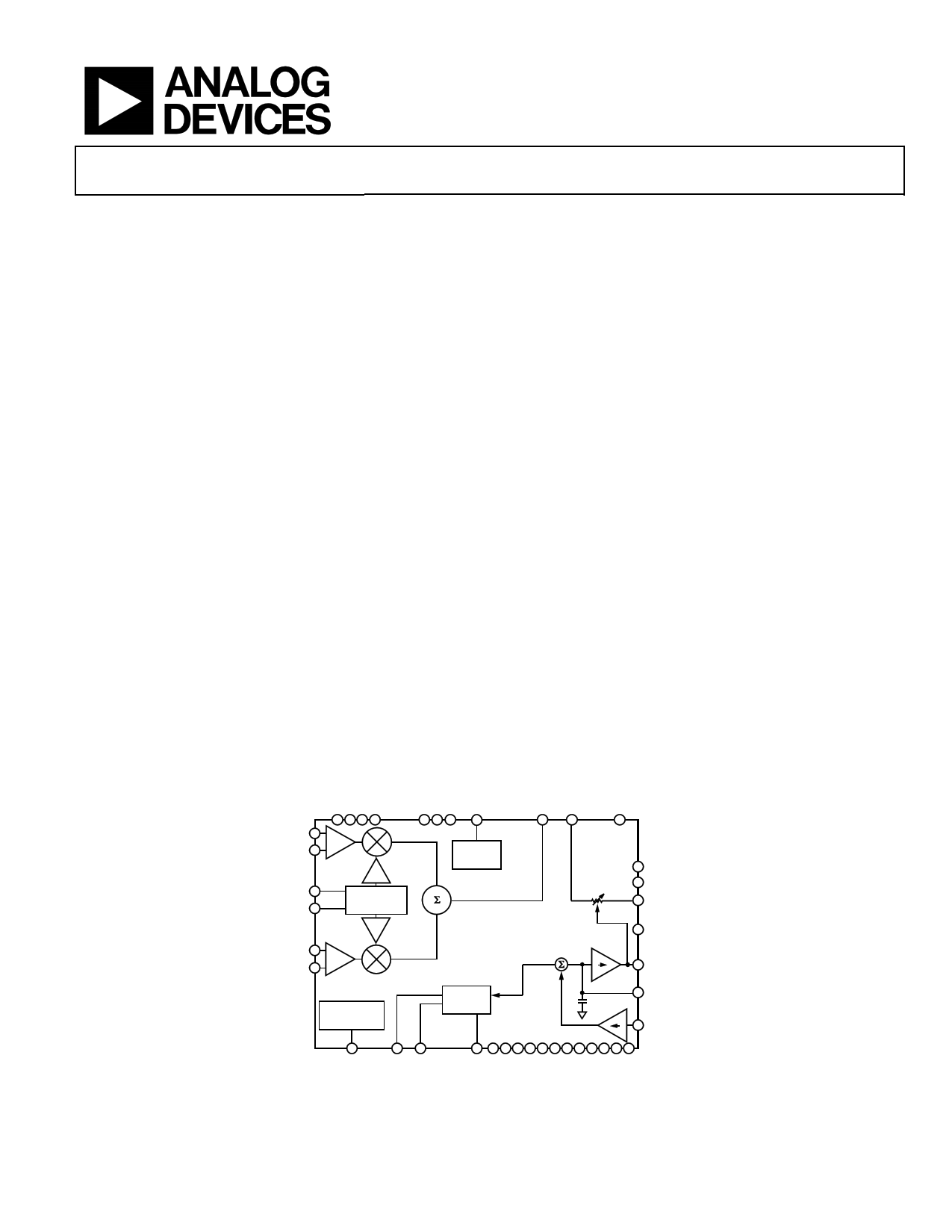
FUNCTIONAL BLOCK DIAGRAM
VPOS
38 37 36 35
VPOS ENBL
23 22 21
24
MODOUT ATTI
10 12
NC
9
QUADRATURE
PHASE
SPLITTER
IQ MOD
BIAS
ADL5386
15dB
17 ATTCM
14 ATTCM
20 ATTO
6 VREF
IV
7 VDET/VCTL
TEMPERATURE
SENSOR
LOG
DETECTOR
4 CLPF
I V 3 VSET
8
TEMP
12
INLO INHI
39 5 11 13 15 16 18 19 27 28 31 32 40
TADJ
COMM
Figure 1.
Rev. 0
Information furnished by Analog Devices is believed to be accurate and reliable. However, no
responsibility is assumed by Analog Devices for its use, nor for any infringements of patents or other
rights of third parties that may result from its use. Specifications subject to change without notice. No
license is granted by implication or otherwise under any patent or patent rights of Analog Devices.
Trademarksandregisteredtrademarksarethepropertyoftheirrespectiveowners.
One Technology Way, P.O. Box 9106, Norwood, MA 02062-9106, U.S.A.
Tel: 781.329.4700
www.analog.com
Fax: 781.461.3113
©2009 Analog Devices, Inc. All rights reserved.
1 page 
ADL5386
Parameter
Sideband Suppression
Quadrature Error
I/Q Amplitude Balance
Second Harmonic
Third Harmonic
Output IP2
Output IP3
Noise Floor
Output Frequency = 860 MHz
Output Power
Modulator Voltage Gain
Output P1dB
Output Return Loss
Carrier Leakage
Sideband Suppression
Quadrature Error
I/Q Amplitude Balance
Second Harmonic
Third Harmonic
Output IP2
Output IP3
Noise Floor
Output Frequency = 1450 MHz
Output Power
Modulator Voltage Gain
Output P1dB
Output Return Loss
Carrier Leakage
Sideband Suppression
Quadrature Error
I/Q Amplitude Balance
Second Harmonic
Third Harmonic
Output IP2
Output IP3
Noise Floor
Conditions
Unadjusted (nominal drive level)
At 85°C after optimization at 25°C
At −40°C after optimization at +25°C
(fLO − (2 × fBB)), POUT = 5 dBm
(fLO + (3 × fBB)), POUT = 5 dBm
F1 = 3.5 MHz, F2 = 4.5 MHz, POUT = −3 dBm per tone
F1 = 3.5 MHz, F2 = 4.5 MHz, POUT = −3 dBm per tone
20 MHz offset from LO, all BB inputs at a bias of 500 mV
20 MHz offset from LO, output power = −5 dBm
Min Typ
−46
−57
−57
−0.5
0.05
−76
−53
74
25
−160
−156
Single (lower) sideband output
Unadjusted (nominal drive level)
At 85°C after optimization at 25°C
At −40°C after optimization at +25°C
Unadjusted (nominal drive level)
At 85°C after optimization at 25°C
At −40°C after optimization at +25°C
(fLO − (2 × fBB)), POUT = 5 dBm
(fLO + (3 × fBB)), POUT = 5 dBm
F1 = 3.5 MHz, F2 = 4.5 MHz, POUT = −3 dBm per tone
F1 = 3.5 MHz, F2 = 4.5 MHz, POUT = −3 dBm per tone
20 MHz offset from LO, all BB inputs at a bias of 500 mV
20 MHz offset from LO, output power = −5 dBm
3.8 5.3
−1.6
11.4
−15
−37
−56
−56
−39
−55
−55
−0.9
0.05
−72
−49
73
25
−160
−157
Single (lower) sideband output
Unadjusted (nominal drive level)
At 85°C after optimization at 25°C
At −40°C after optimization at +25°C
Unadjusted (nominal drive level)
At 85°C after optimization at 25°C
At −40°C after optimization at +25°C
(fLO − (2 × fBB)), POUT = 5 dBm
(fLO + (3 × fBB)), POUT = 5 dBm
F1 = 3.5 MHz, F2 = 4.5 MHz, POUT = −3 dBm per tone
F1 = 3.5 MHz, F2 = 4.5 MHz, POUT = −3 dBm per tone
20 MHz offset from LO, all BB inputs at a bias of 500 mV
4.3
−2.6
10.6
−15
−35
−50
−50
−43
−45
−45
−0.2
0.03
−67
−45
63
25
−160
Max Unit
dBc
dBc
dBc
Degrees
dB
dBc
dBc
dBm
dBm
dBm/Hz
dBm/Hz
6.8 dBm
dB
dBm
dB
dBm
dBm
dBm
dBc
dBc
dBc
Degrees
dB
dBc
dBc
dBm
dBm
dBm/Hz
dBm/Hz
dBm
dB
dBm
dB
dBm
dBm
dBm
dBc
dBc
dBc
Degrees
dB
dBc
dBc
dBm
dBm
dBm/Hz
Rev. 0 | Page 4 of 36
5 Page 
ADL5386
PIN CONFIGURATION AND FUNCTION DESCRIPTIONS
IBBP 25
IBBN 26
VPOS
38 37 36 35
LOIP 33
LOIN 34
QUADRATURE
PHASE
SPLITTER
QBBN 29
QBBP 30
VPOS
23 22 21
ENBL
24
MODOUT ATTI
10 12
NC
9
IQ MOD
BIAS
ADL5386
15dB
17 ATTCM
14 ATTCM
20 ATTO
6 VREF
IV
7 VDET/VCTL
TEMPERATURE
SENSOR
LOG
DETECTOR
4 CLPF
I V 3 VSET
8
TEMP
12
INLO INHI
39 5 11 13 15 16 18 19 27 28 31 32 40
TADJ
COMM
NOTES
1. NC = NO CONNECT.
2. CONNECT THE EXPOSED PAD TO GROUND VIA A LOW IMPEDANCE PATH.
Figure 2. Pin Configuration
Table 4. Pin Function Descriptions
Pin No.
Mnemonic Description
1
INLO
Detector Common. This pin should be ac-coupled to ground.
2 INHI Detector Input. When operating in AGC mode, a portion of the signal at the output of the VVA (or at the
output of a subsequent stage) is coupled back to this input. The signal should be ac-coupled into INHI. To provide
a 50 Ω match at INHI, a 50 Ω resistor should be connected between INHI and ground (with the ac-coupling
capacitor placed between the resistor and the INHI pin).
3
VSET
Setpoint Input. Setpoint input for controller mode or feedback input for measurement mode.
4
CLPF
AGC Loop Filter Capacitor. The ground-referenced capacitor that is connected to this pin sets the loop bandwidth
of the AGC circuit.
5, 11, 13, 15, COMM
16, 18, 19, 27,
28, 31, 32, 40
Device Common. Connect these pins to the same low impedance ground plane.
6
VREF
Attenuator Control Voltage Reference. In AGC mode, this pin should be left open. In open-loop mode, when
the VVA is being controlled externally, a 2 V reference voltage should be applied to this pin.
7 VDET/VCTL Detector Output/VVA Control Voltage Input. When the VVA is being controlled externally (open-loop mode),
the attenuation is controlled by the external voltage applied to this pin. The VVA control range is from 0 V
(maximum attenuation) to 2 V (minimum attenuation). In this mode, VREF (Pin 6) should be tied to approximately
2 V. When the VVA is being operated in AGC mode, this pin is left open with the voltage on the pin representing the
AGC drive voltage to the VVA. If the VVA is not being used, the AGC log amp can be used as a standalone detector
by connecting this pin to VSET. In this mode, the log amp output voltage is available at this pin.
8
TEMP
Temperature Sensor Output. This pin provides a standalone temperature sensor output voltage. At room
temperature, the nominal output voltage is equal to 1.45 V. The slope of the output voltage is equal to 4.6 mV/°C.
9 NC No Connect. Do not connect this pin.
10 MODOUT RF Output of IQ Modulator. Single-ended, 50 Ω internally biased RF output. MODOUT is generally
ac-coupled to the input of the VVA (either ATTI or ATTO).
12, 20
ATTI, ATTO VVA RF Input/Output. ATTI is normally ac-coupled to MODOUT. However, because the VVA is completely reversible,
MODOUT can also drive ATTO with ATTI operating as the VVA output.
14, 17
ATTCM
VVA Input/Output Common. These pins should be ac-coupled to ground.
21 to 23,
35 to 38
VPOS
Power Supply. Positive supply voltage pins. All pins should be connected to the same supply (VS). To ensure
adequate external bypassing, connect a 0.1 μF capacitor between each pin and ground.
Rev. 0 | Page 10 of 36
11 Page | ||
| Páginas | Total 30 Páginas | |
| PDF Descargar | [ Datasheet ADL5386.PDF ] | |
Hoja de datos destacado
| Número de pieza | Descripción | Fabricantes |
| ADL5380 | 400 MHz to 6 GHz Quadrature Demodulator | Analog Devices |
| ADL5382 | 700 MHz to 2.7 GHz Quadrature Demodulator | Analog Devices |
| ADL5385 | Quadrature Modulator | Analog Devices |
| ADL5386 | 50 MHz to 2200 MHz Quadrature Modulator | Analog Devices |
| Número de pieza | Descripción | Fabricantes |
| SLA6805M | High Voltage 3 phase Motor Driver IC. |
Sanken |
| SDC1742 | 12- and 14-Bit Hybrid Synchro / Resolver-to-Digital Converters. |
Analog Devices |
|
DataSheet.es es una pagina web que funciona como un repositorio de manuales o hoja de datos de muchos de los productos más populares, |
| DataSheet.es | 2020 | Privacy Policy | Contacto | Buscar |