|
|
|
PDF AD7476A Data sheet ( Hoja de datos )
| Número de pieza | AD7476A | |
| Descripción | 12-/10-/8-Bit ADC | |
| Fabricantes | Analog Devices | |
| Logotipo | ||
Hay una vista previa y un enlace de descarga de AD7476A (archivo pdf) en la parte inferior de esta página. Total 28 Páginas | ||
|
No Preview Available !
Data Sheet
2.35 V to 5.25 V, 1 MSPS,
12-/10-/8-Bit ADCs in 6-Lead SC70
AD7476A/AD7477A/AD7478A
FEATURES
Fast throughput rate: 1 MSPS
Specified for VDD of 2.35 V to 5.25 V
Low power
3.6 mW at 1 MSPS with 3 V supplies
12.5 mW at 1 MSPS with 5 V supplies
Wide input bandwidth
71 dB SNR at 100 kHz input frequency
Flexible power/serial clock speed management
No pipeline delays
High speed serial interface
SPI/QSPI™/MICROWIRE/DSP compatible
Standby mode: 1 µA maximum
6-lead SC70 package
8-lead MSOP
Qualified for automotive applications
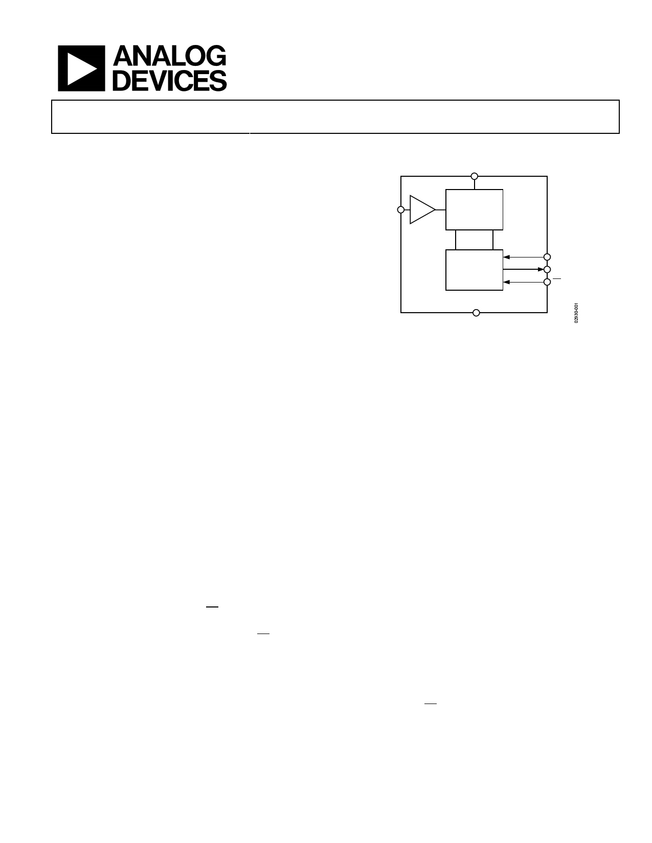
FUNCTIONAL BLOCK DIAGRAM
VDD
VIN T/H
12-/10-/8-BIT
SUCCESSIVE-
APPROXIMATION
ADC
CONTROL
LOGIC
AD7476A/AD7477A/AD7478A
GND
Figure 1.
SCLK
SDATA
CS
APPLICATIONS
Battery-powered systems
Personal digital assistants
Medical instruments
Mobile communications
Instrumentation and control systems
Data acquisition systems
High speed modems
Optical sensors
GENERAL DESCRIPTION
The AD7476A/AD7477A/AD7478A are 12-bit, 10-bit, and 8-bit
high speed, low power, successive-approximation analog-to-
digital converters (ADCs), respectively. The parts operate from
a single 2.35 V to 5.25 V power supply and feature throughput
rates up to 1 MSPS. The parts contain a low noise, wide
bandwidth track-and-hold amplifier that can handle input
frequencies in excess of 13 MHz. The conversion process and
data acquisition are controlled using CS and the serial clock,
allowing the devices to interface with microprocessors or DSPs.
The input signal is sampled on the falling edge of CS, and the
conversion is also initiated at this point. There are no pipeline
delays associated with the parts. The AD7476A/AD7477A/
AD7478A use advanced design techniques to achieve low power
dissipation at high throughput rates. The reference for the part
is taken internally from VDD to allow the widest dynamic input
range to the ADC. Thus, the analog input range for the part is
0 V to VDD. The conversion rate is determined by the SCLK.
PRODUCT HIGHLIGHTS
1. First 12-/10-/8-bit ADCs in a SC70 package.
2. High throughput with low power consumption.
3. Flexible power/serial clock speed management. The
conversion rate is determined by the serial clock, allowing
the conversion time to be reduced through the serial clock
speed increase. This allows the average power consumption
to be reduced when a power-down mode is used while not
converting. The parts also feature a power-down mode to
maximize power efficiency at lower throughput rates.
Current consumption is 1 µA maximum and 50 nA
typically when in power-down mode.
4. Reference derived from the power supply.
5. No pipeline delay. The parts feature a standard successive
approximation ADC with accurate control of the sampling
instant via a CS input and once-off conversion control.
Rev. G
Document Feedback
Information furnished by Analog Devices is believed to be accurate and reliable. However, no
responsibility is assumed by Analog Devices for its use, nor for any infringements of patents or other
rights of third parties that may result from its use. Specifications subject to change without notice. No
license is granted by implication or otherwise under any patent or patent rights of Analog Devices.
Trademarksandregisteredtrademarksarethepropertyoftheirrespectiveowners.
One Technology Way, P.O. Box 9106, Norwood, MA 02062-9106, U.S.A.
Tel: 781.329.4700 ©2002–2016 Analog Devices, Inc. All rights reserved.
Technical Support
www.analog.com
1 page 
Data Sheet
AD7476A/AD7477A/AD7478A
AD7477A SPECIFICATIONS
VDD = 2.35 V to 5.25 V, fSCLK = 20 MHz, fSAMPLE = 1 MSPS, TA = TMIN to TMAX, unless otherwise noted.1
Table 2.
Parameter
DYNAMIC PERFORMANCE
Signal-to-Noise-and-Distortion (SINAD)3
Total Harmonic Distortion (THD)3
Peak Harmonic or Spurious Noise (SFDR)3
Intermodulation Distortion (IMD)3
Second-Order Terms
Third-Order Terms
Aperture Delay
Aperture Jitter
Full Power Bandwidth
DC ACCURACY
Resolution
Integral Nonlinearity
Differential Nonlinearity
Offset Error3, 4
Gain Error3, 4
Total Unadjusted Error (TUE)3, 4
ANALOG INPUT
Input Voltage Range
DC Leakage Current
Input Capacitance
LOGIC INPUTS
Input High Voltage, VINH
Input Low Voltage, VINL
Input Current, IIN, SCLK Pin
Input Current, IIN, CS Pin
Input Capacitance, CIN5
LOGIC OUTPUTS
Output High Voltage VOH
Output Low Voltage, VOL
Floating-State Leakage Current
Floating-State Output Capacitance5
Output Coding
CONVERSION RATE
Conversion Time
Track-and-Hold Acquisition Time3
Throughput Rate
A Grade2 Unit
61 dB min
−72 dB max
−73 dB max
−82 dB typ
−82 dB typ
10 ns typ
30 ps typ
13.5 MHz typ
2 MHz typ
10 Bits
±0.5 LSB max
±0.5 LSB max
±1 LSB max
±1 LSB max
±1.2 LSB max
0 to VDD
±0.5
20
V
µA max
pF typ
2.4 V min
1.8 V min
0.8 V max
0.4 V max
±0.5 μA max
±10 nA typ
5 pF max
VDD − 0.2
V min
0.4 V max
±1 μA max
5 pF max
Straight (Natural) Binary
700 ns max
250 ns max
1 MSPS max
Test Conditions/Comments
fIN = 100 kHz sine wave
fa = 100.73 kHz, fb = 90.7 kHz
fa = 100.73 kHz, fb = 90.7 kHz
At 3 dB
At 0.1 dB
Guaranteed no missed codes to 10 bits
Track-and-hold in track; 6 pF typ when in hold
VDD = 2.35 V
VDD = 5 V
VDD = 3 V
Typically 10 nA, VIN = 0 V or VDD
ISOURCE = 200 μA, VDD = 2.35 V to 5.25 V
ISINK = 200 μA
14 SCLK cycles with SCLK at 20 MHz
Rev. G | Page 5 of 28
5 Page 
Data Sheet
PIN CONFIGURATIONS AND FUNCTION DESCRIPTIONS
AD7476A/AD7477A/AD7478A
VDD 1 AD7476A/ 6 CS
GND 2 AD7477A/ 5 SDATA
AD7478A
VIN 3 TOP VIEW 4 SCLK
(Not to Scale)
Figure 5. 6-Lead SC70 Pin Configuration
VDD 1 AD7476A/ 8 VIN
SDATA 2 AD7477A/ 7 GND
CS 3 AD7478A 6 SCLK
TOP VIEW
NC 4 (Not to Scale) 5 NC
NC = NO CONNECT
Figure 6. 8-Lead MSOP Pin Configuration
Table 6. Pin Function Descriptions
Mnemonic Description
CS Chip Select. Active low logic input. This input provides the dual function of initiating conversions on the
AD7476A/AD7477A/AD7478A and also frames the serial data transfer.
VDD
GND
Power Supply Input. The VDD range for AD7476A/AD7477A/AD7478A is from 2.35 V to 5.25 V.
Analog Ground. Ground reference point for all circuitry on AD7476A/AD7477A/AD7478A. Refer all analog input signals to this
GND voltage.
VIN Analog Input. Single-ended analog input channel. The input range is 0 V to VDD.
SDATA
Data Out. Logic output. The conversion result from AD7476A/AD7477A/AD7478A is provided on this output as a serial data
stream. The bits are clocked out on the falling edge of the SCLK input. The data stream from the AD7476A consists of four
leading zeros followed by 12 bits of conversion data that are provided MSB first. The data stream from the AD7477A consists
of four leading zeros followed by 10 bits of conversion data followed by two trailing zeros, provided MSB first. The data stream
from the AD7478A consists of four leading zeros followed by 8 bits of conversion data followed by four trailing zeros that are
provided MSB first.
SCLK
Serial Clock. Logic input. SCLK provides the serial clock for accessing data from the part. This clock input is also used as the
clock source for the conversion process of AD7476A/AD7477A/AD7478A.
NC No Connect.
Rev. G | Page 11 of 28
11 Page | ||
| Páginas | Total 28 Páginas | |
| PDF Descargar | [ Datasheet AD7476A.PDF ] | |
Hoja de datos destacado
| Número de pieza | Descripción | Fabricantes |
| AD7476 | 1 MSPS/ 12-/10-/8-Bit ADCs in 6-Lead SOT-23 | Analog Devices |
| AD7476A | 2.35 V to 5.25 V/ 1 MSPS/ 12-/10-/8-Bit ADCs in 6-Lead SC70 | Analog Devices |
| AD7476A | 12-/10-/8-Bit ADC | Analog Devices |
| Número de pieza | Descripción | Fabricantes |
| SLA6805M | High Voltage 3 phase Motor Driver IC. |
Sanken |
| SDC1742 | 12- and 14-Bit Hybrid Synchro / Resolver-to-Digital Converters. |
Analog Devices |
|
DataSheet.es es una pagina web que funciona como un repositorio de manuales o hoja de datos de muchos de los productos más populares, |
| DataSheet.es | 2020 | Privacy Policy | Contacto | Buscar |