|
|
PDF ADP5075 Data sheet ( Hoja de datos )
| Número de pieza | ADP5075 | |
| Descripción | DC-to-DC Inverting Regulator | |
| Fabricantes | Analog Devices | |
| Logotipo |  |
|
Hay una vista previa y un enlace de descarga de ADP5075 (archivo pdf) en la parte inferior de esta página. Total 19 Páginas | ||
|
No Preview Available !
Data Sheet
800 mA, DC-to-DC Inverting Regulator
ADP5075
FEATURES
Wide input voltage range: 2.85 V to 15 V
Adjustable negative output to VIN − 39 V
Integrated 800 mA main switch
1.2 MHz/2.4 MHz switching frequency with optional external
frequency synchronization from 1.0 MHz to 2.6 MHz
Resistor programmable soft start timer
Slew rate control for lower system noise
Precision enable control
UVLO, OCP, OVP, and TSD protection
1.61 mm × 2.18 mm, 12-ball WLCSP
−40°C to +125°C junction temperature range
Supported by the ADIsimPower tool set
APPLICATIONS
Bipolar amplifiers, analog-to-digital converters (ADCs),
digital-to-analog converters (DACs), and multiplexers
Charge coupled device (CCD) bias supplies
Optical module supplies
Radio frequency (RF) power amplifier (PA) bias
GENERAL DESCRIPTION
The ADP5075 is a high performance dc-to-dc inverting regulator
used to generate negative supply rails.
The input voltage range of 2.85 V to 15 V supports a wide variety of
applications. The integrated main switch enables the generation of
an adjustable negative output voltage down to 39 V below the input
voltage.
The ADP5075 operates at a pin selected 1.2 MHz/2.4 MHz
switching frequency. The ADP5075 can synchronize with an
external oscillator from 1.0 MHz to 2.6 MHz to ease noise
filtering in sensitive applications. The regulator implements
programmable slew rate control circuitry for the MOSFET
driver stage to reduce electromagnetic interference (EMI).
The ADP5075 includes a fixed internal or resistor programmable
soft start timer to prevent inrush current at power-up. During
shutdown, the regulator completely disconnects the load from the
input supply to provide a true shutdown.
TYPICAL APPLICATION CIRCUIT
VIN
CIN
ON
OFF
RC
CC
CVREG
AVIN
PVIN
VREF
ADP5075 FB
EN
SS SW
COMP
SLEW
VREG SYNC/FREQ
GND
CVREF
RFB
RFT
D1
L1
VOUT
COUT
Figure 1.
Other key safety features in the ADP5075 include overcurrent
protection (OCP), overvoltage protection (OVP), thermal
shutdown (TSD), and input undervoltage lockout (UVLO).
The ADP5075 is available in a 12-ball WLCSP and is rated for a
−40°C to +125°C junction temperature range.
Table 1. Related Devices
Device
Boost
Switch (A)
Inverter
Switch (A)
ADP5070 1.0
0.6
ADP5071 2.0
1.2
ADP5075 Not
applicable
0.8
Package
20-lead LFCSP (4 mm ×
4 mm) and 20-lead TSSOP
20-lead LFCSP (4 mm ×
4 mm) and 20-lead TSSOP
12-ball WLCSP
(1.61 mm × 2.18 mm)
Rev. A
Document Feedback
Information furnished by Analog Devices is believed to be accurate and reliable. However, no
responsibility is assumed by Analog Devices for its use, nor for any infringements of patents or other
rights of third parties that may result from its use. Specifications subject to change without notice. No
license is granted by implication or otherwise under any patent or patent rights of Analog Devices.
Trademarksandregisteredtrademarksarethepropertyoftheirrespectiveowners.
One Technology Way, P.O. Box 9106, Norwood, MA 02062-9106, U.S.A.
Tel: 781.329.4700
©2015 Analog Devices, Inc. All rights reserved.
Technical Support
www.analog.com
1 page 
ADP5075
Parameter
SOFT START
Soft Start Timer
Hiccup Time
THERMAL SHUTDOWN
Threshold
Hysteresis
Symbol
tSS
tHICCUP
TSHDN
THYS
Data Sheet
Min Typ Max Unit Test Conditions/Comments
4
32
8 × tSS
ms SS = open
ms SS resistor = 50 kΩ to GND
ms
150 °C
15 °C
Rev. A | Page 4 of 18
5 Page 
ADP5075
IINDUCTOR
4
2
SW
VNEG
3
CH2 5.00V BW
CH3 20.0mV BW CH4 50.0mA BW
200ns
CH2
T 0.00000s
3.10V
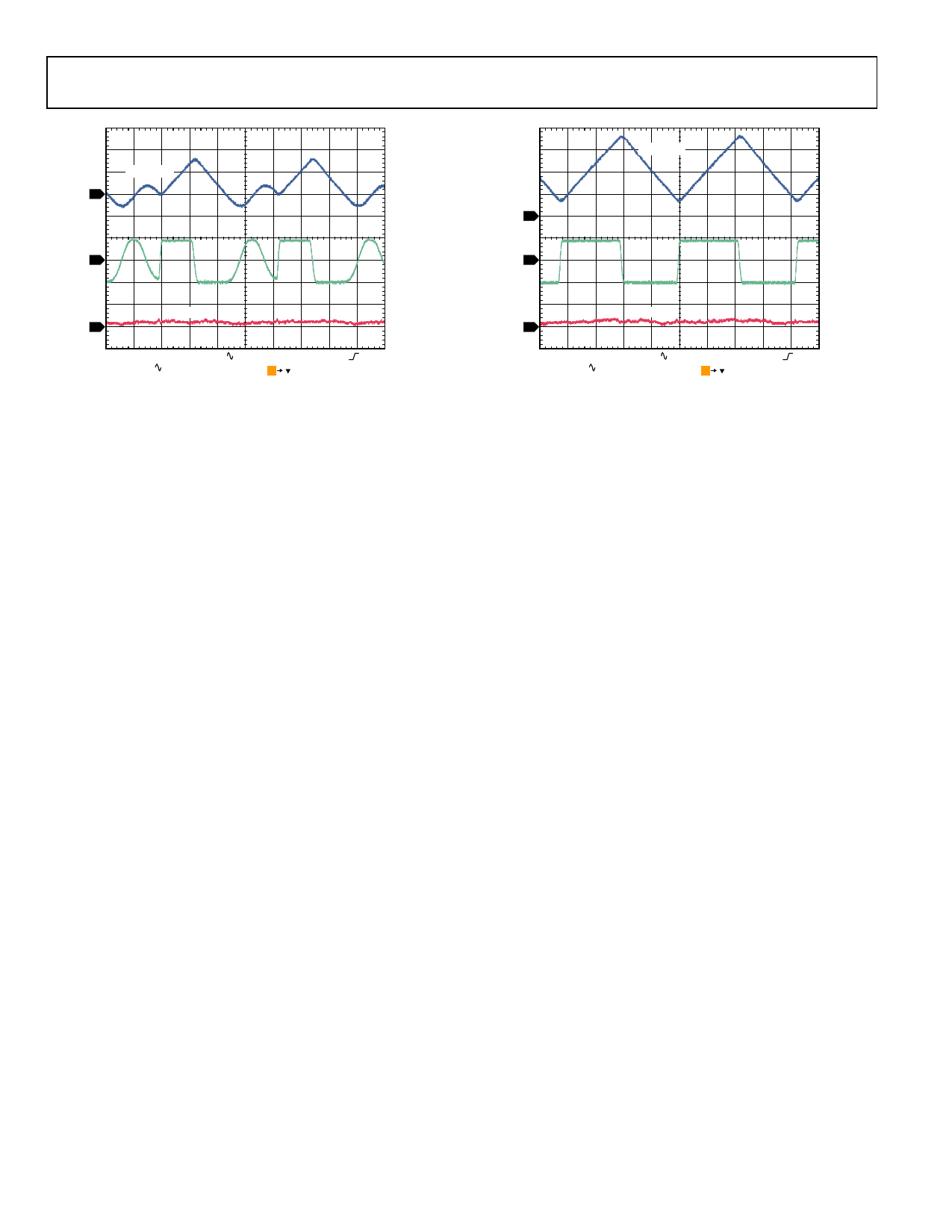
Figure 21. Discontinuous Conduction Mode Operation Showing Inductor
Current (IINDUCTOR), Switch Node Voltage, and Output Ripple, VIN = 5 V,
VNEG = −5 V, ILOAD = 10 mA, fSW = 1.2 MHz, TA = 25°C
IINDUCTOR
Data Sheet
4
2
SW
VNEG
3
CH2 5.00V BW
CH3 20.0mV BW CH4 50.0mA BW
200ns
CH2
T 0.00000s
2.10V
Figure 22. Continuous Conduction Mode Operation Showing Inductor
Current (IINDUCTOR), Switch Node Voltage, and Output Ripple, VIN = 5 V,
VNEG = −5 V, ILOAD = 50 mA, fSW = 1.2 MHz, TA = 25°C
Rev. A | Page 10 of 18
11 Page | ||
| Páginas | Total 19 Páginas | |
| PDF Descargar | [ Datasheet ADP5075.PDF ] | |
Hoja de datos destacado
| Número de pieza | Descripción | Fabricantes |
| ADP5070 | DC-to-DC Switching Regulator | Analog Devices |
| ADP5071 | DC-to-DC Switching Regulator | Analog Devices |
| ADP5073 | DC-to-DC Inverting Regulator | Analog Devices |
| ADP5074 | DC-to-DC Inverting Regulator | Analog Devices |
| Número de pieza | Descripción | Fabricantes |
| SLA6805M | High Voltage 3 phase Motor Driver IC. |
Sanken |
| SDC1742 | 12- and 14-Bit Hybrid Synchro / Resolver-to-Digital Converters. |
Analog Devices |
|
DataSheet.es es una pagina web que funciona como un repositorio de manuales o hoja de datos de muchos de los productos más populares, |
| DataSheet.es | 2020 | Privacy Policy | Contacto | Buscar |
