|
|
|
PDF HMC1121 Data sheet ( Hoja de datos )
| Número de pieza | HMC1121 | |
| Descripción | Power Amplifier | |
| Fabricantes | Analog Devices | |
| Logotipo | ||
Hay una vista previa y un enlace de descarga de HMC1121 (archivo pdf) en la parte inferior de esta página. Total 16 Páginas | ||
|
No Preview Available !
Data Sheet
4 W, GaAs, pHEMT, MMIC
Power Amplifier, 5.5 GHz to 8.5 GHz
HMC1121
FEATURES
High saturated output power (PSAT): 36.5 dBm at 30% power
added efficiency (PAE)
High output third-order intercept (IP3): 44 dBm typical
High gain: 28 dB typical
High output power for 1 dB compression (P1dB): 36 dBm typical
Total supply current: 2200 mA at 7 V
40-lead, 6 mm × 6 mm LFCSP package: 36 mm2
APPLICATIONS
Point to point radios
Point to multipoint radios
Very small aperture terminals (VSATs) and satellite
communications (SATCOMs)
Military electronic warfare (EW) and electronic counter
measures (ECM)
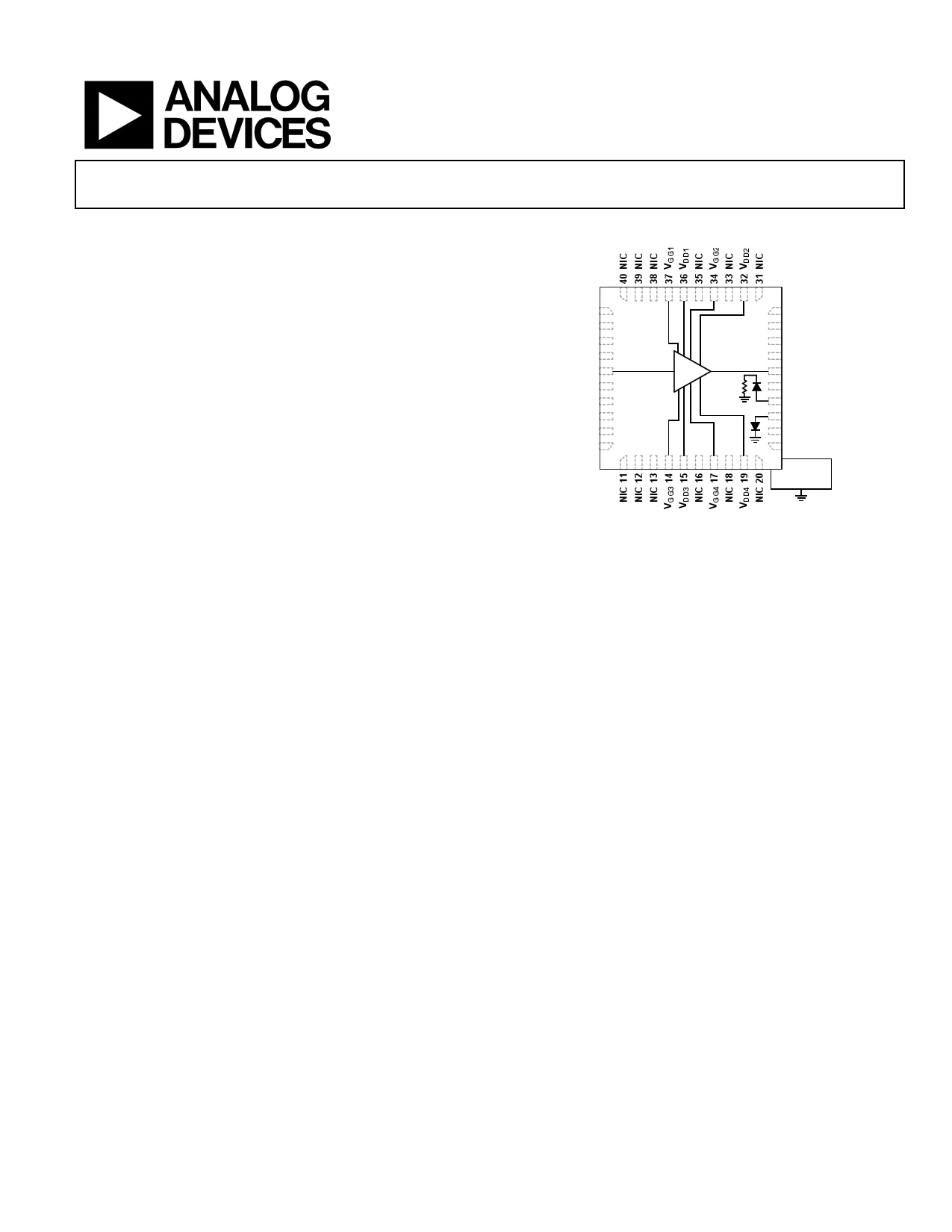
FUNCTIONAL BLOCK DIAGRAM
NIC 1
NIC 2
NIC 3
NIC 4
RFIN 5
NIC 6
NIC 7
NIC 8
NIC 9
NIC 10
HMC1121
30 NIC
29 NIC
28 NIC
27 NIC
26 RFOUT
25 NIC
24 VDET
23 VREF
22 NIC
21 NIC
PACKAGE
BASE
Figure 1.
GENERAL DESCRIPTION
The HMC1121 is a three-stage, gallium arsenide (GaAs),
pseudomorphic high electron mobility transfer (pHEMT),
monolithic microwave integrated circuit (MMIC), 4 W power
amplifier with an integrated temperature compensated on-chip
power detector that operates between 5.5 GHz and 8.5 GHz.
The HMC1121 provides 28 dB of gain, 44 dBm output IP3, and
36.5 dBm of saturated output power at 30% PAE from a 7 V
power supply.
The HMC1121 exhibits excellent linearity and it is optimized
for high capacity, point to point and point to multipoint radio
systems. The amplifier configuration and high gain make it an
excellent candidate for last stage signal amplification preceding
the antenna.
Ideal for supporting higher volume applications, the HMC1121
is provided in a 40-lead LFCSP package.
Rev. 0
Document Feedback
Information furnished by Analog Devices is believed to be accurate and reliable. However, no
responsibility is assumed by Analog Devices for its use, nor for any infringements of patents or other
rights of third parties that may result from its use. Specifications subject to change without notice. No
license is granted by implication or otherwise under any patent or patent rights of Analog Devices.
Trademarksandregisteredtrademarksarethepropertyoftheirrespectiveowners.
One Technology Way, P.O. Box 9106, Norwood, MA 02062-9106, U.S.A.
Tel: 781.329.4700
©2016 Analog Devices, Inc. All rights reserved.
Technical Support
www.analog.com
1 page 
HMC1121
ABSOLUTE MAXIMUM RATINGS
Table 3.
Parameter
Drain Voltage Bias
RF Input Power (RFIN)1
Channel Temperature
Continuous Power Dissipation, PDISS (TA = 85°C,
Derate 227 mW/°C Above 85°C)
Thermal Resistance (RTH) Junction to Ground
Paddle
Maximum Peak Reflow Temperature (MSL3)2
Rating
8V
24 dBm
175°C
20.5 W
4.4°C/W
260°C
Storage Temperature Range
Operating Temperature Range
ESD Sensitivity (Human Body Model)
−65°C to +150°C
−40°C to +85°C
Class 1A,
passed 250 V
1 The maximum input power (PIN) is limited to 24 dBm or to the thermal limits
constrained by the maximum power dissipation.
2 See the Ordering Guide section.
Data Sheet
Stresses at or above those listed under Absolute Maximum
Ratings may cause permanent damage to the product. This is a
stress rating only; functional operation of the product at these
or any other conditions above those indicated in the operational
section of this specification is not implied. Operation beyond
the maximum operating conditions for extended periods may
affect product reliability.
ESD CAUTION
Rev. 0 | Page 4 of 15
5 Page 
HMC1121
40
35
30
25
GAIN
P1dB
PSAT
20
6.0
6.5 7.0 7.5
VDD (V)
8.0
Figure 27. Gain, P1dB, and PSAT vs. Supply Voltage (VDD) at 7 GHz
20
18
16
14
12 5.5GHz
6.5GHz
7.5GHz
8.5GHz
10
–14 –12 –10 –8 –6 –4 –2 0 2 4 6 8 10 12
INPUT POWER (dBm)
Figure 28. Power Dissipation vs. Input Power at TA = 85°C
0
–10
+85°C
+25°C
–40°C
–20
–30
–40
–50
–60
–70
–80
–90
5
678
FREQUENCY (GHz)
9
Figure 29. Reverse Isolation vs. Frequency at Various Temperatures
10
5.5GHz
7.0GHz
8.5GHz
1
Data Sheet
0.1
0.01
0.001
–10
0 10 20 30
OUTPUT POWER (dBm)
40
Figure 30. Detector Voltage (VREF − VDET) vs. Output Power at
Various Frequencies
10
+85°C
+25°C
–40°C
1
0.1
0.01
0.001
–10
0 10 20 30
OUTPUT POWER (dBm)
40
Figure 31. Detector Voltage (VREF − VDET) vs. Output Power at Various
Temperatures, at 7 GHz
Rev. 0 | Page 10 of 15
11 Page | ||
| Páginas | Total 16 Páginas | |
| PDF Descargar | [ Datasheet HMC1121.PDF ] | |
Hoja de datos destacado
| Número de pieza | Descripción | Fabricantes |
| HMC1120LP4E | RMS POWER DETECTOR & ENVELOPE TRACKER | Hittite |
| HMC1121 | Power Amplifier | Analog Devices |
| HMC1122 | Silicon Digital Attenuator | Analog Devices |
| HMC1126 | GaAs pHEMT MMIC POWER AMPLIFIER | Hittite |
| Número de pieza | Descripción | Fabricantes |
| SLA6805M | High Voltage 3 phase Motor Driver IC. |
Sanken |
| SDC1742 | 12- and 14-Bit Hybrid Synchro / Resolver-to-Digital Converters. |
Analog Devices |
|
DataSheet.es es una pagina web que funciona como un repositorio de manuales o hoja de datos de muchos de los productos más populares, |
| DataSheet.es | 2020 | Privacy Policy | Contacto | Buscar |