|
|
PDF ADA4304-3 Data sheet ( Hoja de datos )
| Número de pieza | ADA4304-3 | |
| Descripción | Active RF Splitters | |
| Fabricantes | Analog Devices | |
| Logotipo |  |
|
Hay una vista previa y un enlace de descarga de ADA4304-3 (archivo pdf) en la parte inferior de esta página. Total 11 Páginas | ||
|
No Preview Available !
Data Sheet
1:3 and 1:4 Single-Ended, Low Cost,
Active RF Splitters
ADA4304-3/ADA4304-4
FEATURES
Ideal for CATV and terrestrial applications
2.4 GHz, −3 dB bandwidth
1 dB flatness: 54 MHz to 865 MHz
Low noise figure: 4.6 dB
Low distortion
Composite second-order (CSO): −62 dBc
Composite triple beat (CTB): −72 dBc
Nominal 3 dB gain per output channel
25 dB output-to-output isolation, 50 MHz to 1000 MHz
75 Ω input and outputs
Small package size: 16-lead, 3 mm × 3 mm LFCSP
APPLICATIONS
Set-top boxes
Residential gateways
CATV distribution systems
Splitter modules
Digital cable ready (DCR) TVs
FUNCTIONAL BLOCK DIAGRAMS
5V 5V
0.1µF
0.1µF
1µH
VCC
IL
0.01µF
VIN ADA4304-3
GND
VOUT1
VOUT2
VOUT3
0.01µF
0.01µF
0.01µF
Figure 1.
5V 5V
0.1µF
0.1µF
1µH
VCC
IL
0.01µF
VIN ADA4304-4
GND
VOUT1
VOUT2
VOUT3
VOUT4
0.01µF
0.01µF
0.01µF
0.01µF
GENERAL DESCRIPTION
The ADA4304-3/ADA4304-4 are 75 Ω active splitters for use in
applications where a lossless signal split is required. Typical
applications include multituner digital set-top boxes, cable
splitter modules, multituners/digital cable ready (DCR)
televisions, and home gateways where traditional solutions
require discrete passive splitter modules with separate fixed
gain amplifiers.
Figure 2.
The ADA4304-3/ADA4304-4 are fabricated using the
Analog Devices, Inc., proprietary silicon germanium (SiGe),
complementary bipolar process, enabling them to achieve very
low levels of distortion with a noise figure of 4.6 dB. The parts
provide low cost alternatives that simplify designs and improve
system performance by integrating a signal splitter element and
a gain block into a single IC. The ADA4304-3/ADA4304-4 are
available in a 16-lead LFCSP and operate in the extended
industrial temperature range of −40°C to +85°C.
Rev. A
Document Feedback
Information furnished by Analog Devices is believed to be accurate and reliable. However, no
responsibility is assumed by Analog Devices for its use, nor for any infringements of patents or other
rights of third parties that may result from its use. Specifications subject to change without notice. No
license is granted by implication or otherwise under any patent or patent rights of Analog Devices.
Trademarksandregisteredtrademarksarethepropertyoftheirrespectiveowners.
One Technology Way, P.O. Box 9106, Norwood, MA 02062-9106, U.S.A.
Tel: 781.329.4700 ©2007–2016 Analog Devices, Inc. All rights reserved.
Technical Support
www.analog.com
1 page 
Data Sheet
PIN CONFIGURATIONS AND FUNCTION DESCRIPTIONS
ADA4304-3/ADA4304-4
VCC 1
VCC 2
GND 3
VIN 4
ADA4304-3
TOP VIEW
(Not to Scale)
12 VOUT2
11 GND
10 VOUT3
9 GND
VCC 1
VCC 2
GND 3
VIN 4
ADA4304-4
TOP VIEW
(Not to Scale)
12 VOUT2
11 GND
10 VOUT3
9 GND
NOTES
1. NIC = NO INTERNAL CONNECTION.
2. EPAD SHOULD BE CONNECTED TO GND.
Figure 4. ADA4304-3Pin Configuration
Table 4. ADA4304-3 Pin Function Descriptions
Pin No. Mnemonic Description
1, 2, 15,
16
VCC
Supply Pin.
3, 5 to 7,
9, 11
GND
Ground.
4 VIN Input.
8 NIC No Internal Connection.
10
VOUT3
Output 3.
12
VOUT2
Output 2.
13
VOUT1
Output 1.
14 IL
Bias Pin.
EPAD
Exposed Pad. Exposed pad should be
connected to GND.
NOTES
1. EPAD SHOULD BE CONNECTED TO GND.
Figure 5. ADA4304-4 Pin Configuration
Table 5. ADA4304-4 Pin Function Descriptions
Pin No. Mnemonic Description
1, 2, 15, 16 VCC
Supply Pin.
3, 5 to 7,
9, 11
GND
Ground.
4 VIN Input.
8
VOUT4
Output 4.
10
VOUT3
Output 3.
12
VOUT2
Output 2.
13
VOUT1
Output 1.
14 IL
Bias Pin.
EPAD
Exposed Pad. Exposed pad should be
connected to GND.
Rev. A | Page 5 of 11
5 Page 
Data Sheet
ADA4304-3/ADA4304-4
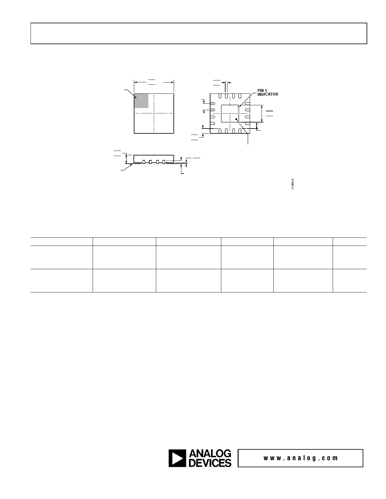
OUTLINE DIMENSIONS
PIN 1
INDICATOR
0.80
0.75
0.70
SEATING
PLANE
3.10
3.00 SQ
2.90
TOP VIEW
0.50
BSC
0.30
0.23
0.18
13
12
16
1
EXPOSED
PAD
PIN 1
INDICATOR
1.45
1.30 SQ
1.15
0.50
0.40
94
85
BOTTOM VIEW
0.25 MIN
0.30
0.05 MAX
0.02 NOM
COPLANARITY
0.08
0.20 REF
FOR PROPER CONNECTION OF
THE EXPOSED PAD, REFER TO
THE PIN CONFIGURATION AND
FUNCTION DESCRIPTIONS
SECTION OF THIS DATA SHEET.
COMPLIANT TO JEDEC STANDARDS MO-220-WEED.
Figure 21. 16-Lead Lead Frame Chip Scale Package [LFCSP]
3 mm × 3 mm Body and 0.75 mm Package Height
(CP-16-21)
Dimensions shown in millimeters
ORDERING GUIDE
Model1
ADA4304-3ACPZ-RL
ADA4304-3ACPZ-R7
ADA4304-3ACPZ-R2
ADA4304-4ACPZ-RL
ADA4304-4ACPZ-R7
ADA4304-4ACPZ-R2
Temperature Range
−40°C to +85°C
−40°C to +85°C
−40°C to +85°C
−40°C to +85°C
−40°C to +85°C
−40°C to +85°C
1 Z=RoHS Compliant Part
Package Description
16-Lead LFCSP
16-Lead LFCSP
16-Lead LFCSP
16-Lead LFCSP
16-Lead LFCSP
16-Lead LFCSP
Package Option
CP-16-21
CP-16-21
CP-16-21
CP-16-21
CP-16-21
CP-16-21
Ordering Quantity
5,000
1,500
250
5,000
1,500
250
Branding
H16
H16
H16
H10
H10
H10
©2007–2016 Analog Devices, Inc. All rights reserved. Trademarks and
registered trademarks are the property of their respective owners.
D07082-0-7/16(A)
Rev. A | Page 11 of 11
11 Page | ||
| Páginas | Total 11 Páginas | |
| PDF Descargar | [ Datasheet ADA4304-3.PDF ] | |
Hoja de datos destacado
| Número de pieza | Descripción | Fabricantes |
| ADA4304-2 | 1:2 Single-Ended Low Cost Active RF Splitter | Analog Devices |
| ADA4304-3 | Active RF Splitters | Analog Devices |
| ADA4304-4 | Active RF Splitters | Analog Devices |
| Número de pieza | Descripción | Fabricantes |
| SLA6805M | High Voltage 3 phase Motor Driver IC. |
Sanken |
| SDC1742 | 12- and 14-Bit Hybrid Synchro / Resolver-to-Digital Converters. |
Analog Devices |
|
DataSheet.es es una pagina web que funciona como un repositorio de manuales o hoja de datos de muchos de los productos más populares, |
| DataSheet.es | 2020 | Privacy Policy | Contacto | Buscar |
