|
|
|
PDF ADuM1301 Data sheet ( Hoja de datos )
| Número de pieza | ADuM1301 | |
| Descripción | Triple-Channel Digital Isolators | |
| Fabricantes | Analog Devices | |
| Logotipo | ||
Hay una vista previa y un enlace de descarga de ADuM1301 (archivo pdf) en la parte inferior de esta página. Total 30 Páginas | ||
|
No Preview Available !
Data Sheet
Triple-Channel Digital Isolators
ADuM1300/ADuM1301
FEATURES
GENERAL DESCRIPTION
Qualified for automotive applications
Low power operation
5 V operation
1.2 mA per channel maximum at 0 Mbps to 2 Mbps
3.5 mA per channel maximum at 10 Mbps
32 mA per channel maximum at 90 Mbps
3 V operation
0.8 mA per channel maximum at 0 Mbps to 2 Mbps
2.2 mA per channel maximum at 10 Mbps
20 mA per channel maximum at 90 Mbps
Bidirectional communication
3 V/5 V level translation
High temperature operation: 125°C
High data rate: dc to 90 Mbps (NRZ)
Precise timing characteristics
2 ns maximum pulse width distortion
2 ns maximum channel-to-channel matching
High common-mode transient immunity: >25 kV/μs
Output enable function
16-lead SOIC wide body package
RoHS-compliant models available
Safety and regulatory approvals
UL recognition: 2500 V rms for 1 minute per UL 1577
CSA Component Acceptance Notice 5A
VDE Certificate of Conformity
DIN V VDE V 0884-10 (VDE V 0884-10):2006-12
VIORM = 560 V peak
TÜV approval: IEC/EN/UL/CSA 61010-1
APPLICATIONS
General-purpose multichannel isolation
SPI interface/data converter isolation
RS-232/RS-422/RS-485 transceivers
Industrial field bus isolation
Automotive systems
The ADuM1300/ADuM13011 are triple-channel digital isolators
based on the Analog Devices, Inc., iCoupler® technology.
Combining high speed CMOS and monolithic transformer
technology, these isolation components provide outstanding
performance characteristics superior to alternatives, such as
optocouplers.
By avoiding the use of LEDs and photodiodes, iCoupler
devices remove the design difficulties commonly associated
with optocouplers. The typical optocoupler concerns regarding
uncertain current transfer ratios, nonlinear transfer functions, and
temperature and lifetime effects are eliminated with the simple
iCoupler digital interfaces and stable performance characteristics.
The need for external drivers and other discrete components is
eliminated with these iCoupler products. Furthermore, iCoupler
devices consume one-tenth to one-sixth of the power of
optocouplers at comparable signal data rates.
The ADuM1300/ADuM1301 isolators provide three independent
isolation channels in a variety of channel configurations and
data rates (see the Ordering Guide). Both models operate with
the supply voltage on either side ranging from 2.7 V to 5.5 V,
providing compatibility with lower voltage systems as well as
enabling a voltage translation functionality across the isolation
barrier. In addition, the ADuM1300/ADuM1301 provide low
pulse width distortion (<2 ns for CRW grade) and tight channel-
to-channel matching (<2 ns for CRW grade). Unlike other
optocoupler alternatives, the ADuM1300/ADuM1301 isolators
have a patented refresh feature that ensures dc correctness in the
absence of input logic transitions and when power is not applied
to one of the supplies.
1 Protected by U.S. Patents 5,952,849; 6,873,065; 6,903,578; and 7,075,329.
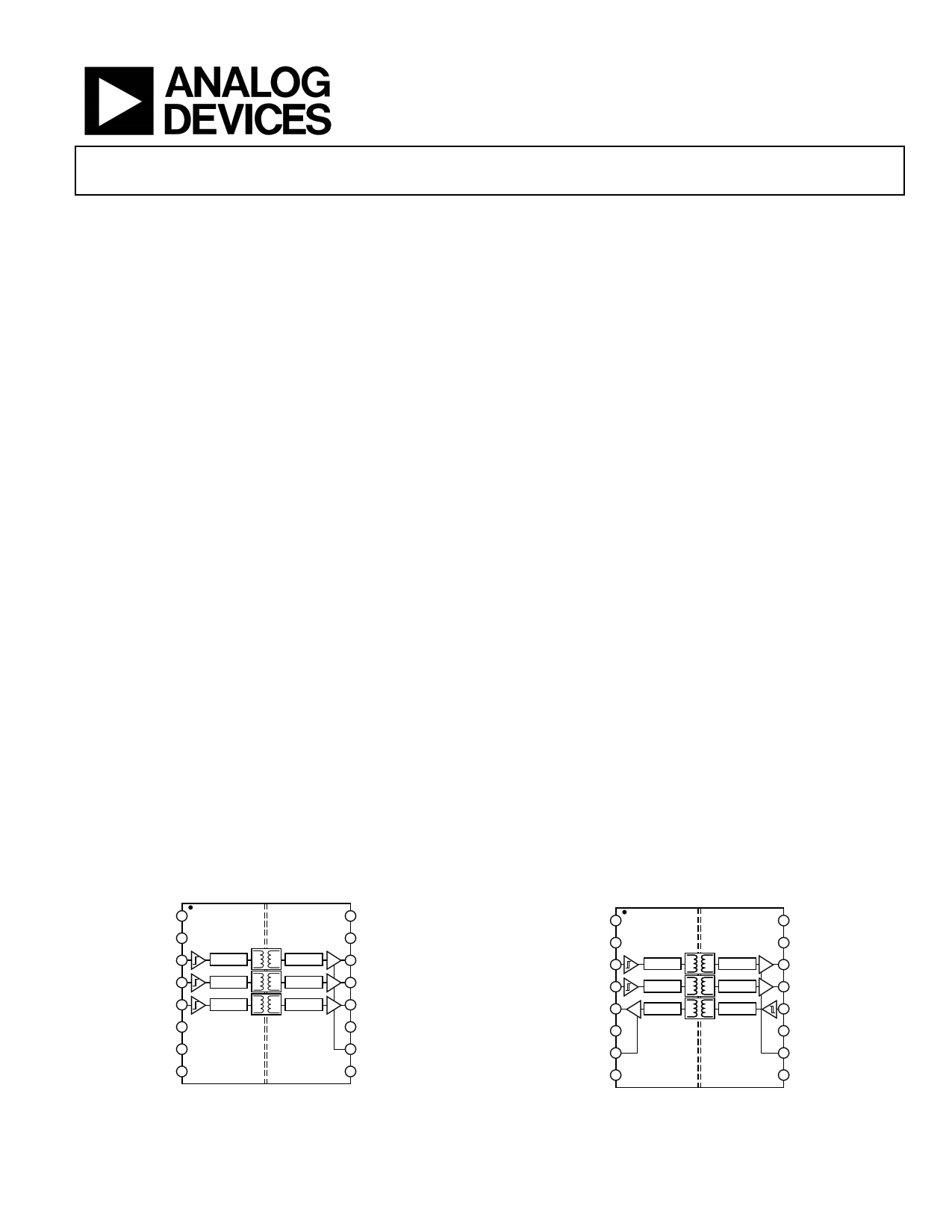
FUNCTIONAL BLOCK DIAGRAMS
VDD1 1
GND1 2
VIA 3
VIB 4
ENCODE
ENCODE
DECODE
DECODE
16 VDD2
15 GND2
14 VOA
13 VOB
VIC 5
ENCODE
DECODE
12 VOC
NC 6
11 NC
NC 7
10 VE2
GND1 8
9 GND2
Figure 1. ADuM1300 Functional Block Diagram
Rev. K
Document Feedback
Information furnished by Analog Devices is believed to be accurate and reliable. However, no
responsibility is assumed by Analog Devices for its use, nor for any infringements of patents or other
rights of third parties that may result from its use. Specifications subject to change without notice. No
license is granted by implication or otherwise under any patent or patent rights of Analog Devices.
Trademarksandregisteredtrademarksarethepropertyoftheirrespectiveowners.
VDD1 1
GND1 2
VIA 3
VIB 4
VOC 5
NC 6
ENCODE
ENCODE
DECODE
DECODE
DECODE
ENCODE
16 VDD2
15 GND2
14 VOA
13 VOB
12 VIC
11 NC
VE1 7
10 VE2
GND1 8
9 GND2
Figure 2. ADuM1301 Functional Block Diagram
One Technology Way, P.O. Box 9106, Norwood, MA 02062-9106, U.S.A.
Tel: 781.329.4700 ©2003–2015 Analog Devices, Inc. All rights reserved.
Technical Support
www.analog.com
1 page 
Data Sheet
ADuM1300/ADuM1301
Parameter
ADuM1300BRW/ADuM1301BRW
Minimum Pulse Width2
Maximum Data Rate3
Propagation Delay4
Pulse Width Distortion, |tPLH − tPHL|4
Change vs. Temperature
Propagation Delay Skew5
Channel-to-Channel Matching, Codirectional
Channels6
Channel-to-Channel Matching, Opposing-
Directional Channels6
ADuM1300CRW/ADuM1301CRW
Minimum Pulse Width2
Maximum Data Rate3
Propagation Delay4
Pulse Width Distortion, |tPLH − tPHL|4
Change vs. Temperature
Propagation Delay Skew5
Channel-to-Channel Matching, Codirectional
Channels6
Channel-to-Channel Matching, Opposing-
Directional Channels6
For All Models
Output Disable Propagation Delay (High/Low
to High Impedance)
Output Enable Propagation Delay (High
Impedance to High/Low)
Output Rise/Fall Time (10% to 90%)
Common-Mode Transient Immunity at Logic
High Output7
Common-Mode Transient Immunity at Logic
Low Output7
Refresh Rate
Input Dynamic Supply Current per Channel8
Output Dynamic Supply Current per Channel8
Symbol
PW
tPHL, tPLH
PWD
tPSK
tPSKCD
tPSKOD
PW
tPHL, tPLH
PWD
tPSK
tPSKCD
tPSKOD
tPHZ, tPLH
tPZH, tPZL
tR/tF
|CMH|
|CML|
fr
IDDI (D)
IDDO (D)
Min
10
20
90
18
25
25
Typ Max Unit
100 ns
Mbps
32 50 ns
3 ns
5 ps/°C
15 ns
3 ns
6 ns
Test Conditions
CL = 15 pF, CMOS signal levels
CL = 15 pF, CMOS signal levels
CL = 15 pF, CMOS signal levels
CL = 15 pF, CMOS signal levels
CL = 15 pF, CMOS signal levels
CL = 15 pF, CMOS signal levels
CL = 15 pF, CMOS signal levels
CL = 15 pF, CMOS signal levels
8.3 11.1 ns
120 Mbps
27 32 ns
0.5 2 ns
3 ps/°C
10 ns
2 ns
5 ns
CL = 15 pF, CMOS signal levels
CL = 15 pF, CMOS signal levels
CL = 15 pF, CMOS signal levels
CL = 15 pF, CMOS signal levels
CL = 15 pF, CMOS signal levels
CL = 15 pF, CMOS signal levels
CL = 15 pF, CMOS signal levels
CL = 15 pF, CMOS signal levels
68
68
2.5
35
35
1.2
0.19
0.05
ns CL = 15 pF, CMOS signal levels
ns CL = 15 pF, CMOS signal levels
ns
kV/µs
CL = 15 pF, CMOS signal levels
VIx = VDD1 or VDD2, VCM = 1000 V,
transient magnitude = 800 V
kV/µs
VIx = 0 V, VCM = 1000 V,
transient magnitude = 800 V
Mbps
mA/Mbps
mA/Mbps
1 The supply current values are for all three channels combined when running at identical data rates. Output supply current values are specified with no output load
present. The supply current associated with an individual channel operating at a given data rate may be calculated as described in the Power Consumption section.
See Figure 6 through Figure 8 for information on per-channel supply current as a function of data rate for unloaded and loaded conditions. See Figure 9 through
Figure 12 for total VDD1 and VDD2 supply currents as a function of data rate for ADuM1300/ADuM1301 channel configurations.
2 The minimum pulse width is the shortest pulse width at which the specified pulse width distortion is guaranteed.
3 The maximum data rate is the fastest data rate at which the specified pulse width distortion is guaranteed.
4 tPHL propagation delay is measured from the 50% level of the falling edge of the VIx signal to the 50% level of the falling edge of the VOx signal. tPLH propagation delay is
measured from the 50% level of the rising edge of the VIx signal to the 50% level of the rising edge of the VOx signal.
5 tPSK is the magnitude of the worst-case difference in tPHL or tPLH that is measured between units at the same operating temperature, supply voltages, and output load
within the recommended operating conditions.
6 Codirectional channel-to-channel matching is the absolute value of the difference in propagation delays between any two channels with inputs on the same side of
the isolation barrier. Opposing-directional channel-to-channel matching is the absolute value of the difference in propagation delays between any two channels with
inputs on opposing sides of the isolation barrier.
7 CMH is the maximum common-mode voltage slew rate that can be sustained while maintaining VO > 0.8 VDD2. CML is the maximum common-mode voltage slew rate
that can be sustained while maintaining VO < 0.8 V. The common-mode voltage slew rates apply to both rising and falling common-mode voltage edges. The transient
magnitude is the range over which the common mode is slewed.
8 Dynamic supply current is the incremental amount of supply current required for a 1 Mbps increase in signal data rate. See Figure 6 through Figure 8 for information
on per-channel supply current for unloaded and loaded conditions. See the Power Consumption section for guidance on calculating the per-channel supply current
for a given data rate.
Rev. K | Page 5 of 32
5 Page 
Data Sheet
ADuM1300/ADuM1301
ELECTRICAL CHARACTERISTICS—5 V, 125°C OPERATION
All voltages are relative to their respective ground. 4.5 V ≤ VDD1 ≤ 5.5 V, 4.5 V ≤ VDD2 ≤ 5.5 V; all minimum/maximum specifications apply
over the entire recommended operation range, unless otherwise noted; all typical specifications are at TA = 25°C, VDD1 = VDD2 = 5 V. These
specifications apply to ADuM1300W and ADuM1301W automotive grade versions.
Table 4.
Parameter
Symbol
DC SPECIFICATIONS
Input Supply Current per Channel, Quiescent
IDDI (Q)
Output Supply Current per Channel, Quiescent IDDO (Q)
ADuM1300W, Total Supply Current, Three Channels1
DC to 2 Mbps
VDD1 Supply Current
IDD1 (Q)
VDD2 Supply Current
IDD2 (Q)
10 Mbps (TRWZ Grade Only)
VDD1 Supply Current
IDD1 (10)
VDD2 Supply Current
IDD2 (10)
ADuM1301W, Total Supply Current, Three Channels1
DC to 2 Mbps
VDD1 Supply Current
IDD1 (Q)
VDD2 Supply Current
IDD2 (Q)
10 Mbps (TRWZ Grade Only)
VDD1 Supply Current
IDD1 (10)
VDD2 Supply Current
IDD2 (10)
For All Models
Input Currents
IIA, IIB, IIC, IE1, IE2
Min
−10
Typ Max Unit
0.50 0.53 mA
0.19 0.24 mA
1.6 2.5 mA
0.7 1.0 mA
6.5 8.1 mA
1.9 2.5 mA
1.3 2.1 mA
1.0 1.4 mA
5.0 6.2 mA
3.4 4.2 mA
+0.01 +10 µA
Logic High Input Threshold
Logic Low Input Threshold
Logic High Output Voltages
Logic Low Output Voltages
SWITCHING SPECIFICATIONS
ADuM1300WSRWZ/ADuM1301WSRWZ
Minimum Pulse Width2
Maximum Data Rate3
Propagation Delay4
Pulse Width Distortion, |tPLH − tPHL|4
Propagation Delay Skew5
Channel-to-Channel Matching6
ADuM1300WTRWZ/ADuM1301WTRWZ
Minimum Pulse Width2
Maximum Data Rate3
Propagation Delay4
Pulse Width Distortion, |tPLH − tPHL|4
Change vs. Temperature
Propagation Delay Skew5
Channel-to-Channel Matching, Codirectional
Channels6
Channel-to-Channel Matching, Opposing-
Directional Channels6
VIH, VEH
VIL, VEL
VOAH, VOBH, VOCH
VOAL, VOBL, VOCL
2.0
VDD1, VDD2 − 0.1
VDD1, VDD2 − 0.4
5.0
4.8
0.0
0.04
0.2
0.8
0.1
0.1
0.4
V
V
V
V
V
V
V
PW
tPHL, tPLH
PWD
tPSK
tPSKCD/tPSKOD
PW
tPHL, tPLH
PWD
tPSK
tPSKCD
tPSKOD
1
50
10
18
1000 ns
Mbps
65 100 ns
40 ns
50 ns
50 ns
100 ns
Mbps
27 32 ns
3 ns
5 ps/°C
15 ns
3 ns
6 ns
Test Conditions
DC to 1 MHz logic signal freq.
DC to 1 MHz logic signal freq.
5 MHz logic signal freq.
5 MHz logic signal freq.
DC to 1 MHz logic signal freq.
DC to 1 MHz logic signal freq.
5 MHz logic signal freq.
5 MHz logic signal freq.
0 V ≤ VIA, VIB, VIC ≤ VDD1 or VDD2,
0 V ≤ VE1, VE2 ≤ VDD1 or VDD2
IOx = −20 µA, VIx = VIxH
IOx = −4 mA, VIx = VIxH
IOx = 20 µA, VIx = VIxL
IOx = 400 µA, VIx = VIxL
IOx = 4 mA, VIx = VIxL
CL = 15 pF, CMOS signal levels
CL = 15 pF, CMOS signal levels
CL = 15 pF, CMOS signal levels
CL = 15 pF, CMOS signal levels
CL = 15 pF, CMOS signal levels
CL = 15 pF, CMOS signal levels
CL = 15 pF, CMOS signal levels
CL = 15 pF, CMOS signal levels
CL = 15 pF, CMOS signal levels
CL = 15 pF, CMOS signal levels
CL = 15 pF, CMOS signal levels
CL = 15 pF, CMOS signal levels
CL = 15 pF, CMOS signal levels
CL = 15 pF, CMOS signal levels
Rev. K | Page 11 of 32
11 Page | ||
| Páginas | Total 30 Páginas | |
| PDF Descargar | [ Datasheet ADuM1301.PDF ] | |
Hoja de datos destacado
| Número de pieza | Descripción | Fabricantes |
| ADuM1300 | Triple-Channel Digital Isolators | Analog Devices |
| ADuM1301 | Triple-Channel Digital Isolators | Analog Devices |
| ADuM130D | 3.0 kV RMS/3.75 kV RMS Triple-Channel Digital Isolators | Analog Devices |
| ADuM130E | 3.0 kV RMS/3.75 kV RMS Triple-Channel Digital Isolators | Analog Devices |
| Número de pieza | Descripción | Fabricantes |
| SLA6805M | High Voltage 3 phase Motor Driver IC. |
Sanken |
| SDC1742 | 12- and 14-Bit Hybrid Synchro / Resolver-to-Digital Converters. |
Analog Devices |
|
DataSheet.es es una pagina web que funciona como un repositorio de manuales o hoja de datos de muchos de los productos más populares, |
| DataSheet.es | 2020 | Privacy Policy | Contacto | Buscar |