|
|
PDF ADS-947 Data sheet ( Hoja de datos )
| Número de pieza | ADS-947 | |
| Descripción | 10MHz Sampling A/D Converters | |
| Fabricantes | Datel | |
| Logotipo |  |
|
Hay una vista previa y un enlace de descarga de ADS-947 (archivo pdf) en la parte inferior de esta página. Total 9 Páginas | ||
|
No Preview Available !
FEATURES
14-bit resolution
10MHz minimum sampling rate
No missing codes
Ideal for both time and frequency-domain
applications
Edge-triggered
Small, 24-pin, ceramic DDIP or SMT
Requires only +5V supplies
Low-power, 2.2 Watts
BLOCK DIAGRAM
ADS-947
14-Bit, 10MHz Sampling A/D Converters
PRODUCT OVERVIEW
The ADS-947 is a 14-bit, 10MHz sampling A/D
converter. This device accurately samples full-scale
input signals up to Nyquist frequencies with no
missing codes. Excellent differential nonlinearity
error (DNL), signal-to-noise ratio (SNR), and total
harmonic distortion (THD) make the ADS-947
the ideal choice for both time-domain (CCD/FPA
imaging, scanners, process control) and frequency-
domain (radar, telecommunications, spectrum
analysis) applications.
The functionally complete ADS-947 contains
a fast-settling sample/hold amplifier, a subranging
(two-pass) A/D converter, an internal reference,
timing/control logic, and error-correction circuitry.
Digital input and output levels are TTL. The ADS-
947 only requires the rising edge of a start convert
pulse to operate.
Requiring only +5V and –5V supplies, the ADS-
947 typically dissipates just 2.2 Watts. The device
is offered with a bipolar input range of ±2V. Models
are available for use in either commercial (0 to
+70°C) or industrial (–40 to +100°C), operating
temperature ranges. A proprietary, auto-calibrating,
error-correcting circuit allows the device to achieve
specified performance over the extended tempera-
ture range.
INPUT/OUTPUT CONNECTIONS
PIN FUNCTION
PIN FUNCTION
1 BIT 1 (MSB)
24 ANALOG GROUND
2 BIT 2
23 OFFSET ADJUST
3 BIT 3
22 +5V ANALOG SUPPLY
4 BIT 4
21 ANALOG INPUT
5 BIT 5
20 –5V SUPPLY
6 BIT 6
19 ANALOG GROUND
7 BIT 7
18 START CONVERT
8 BIT 8
17 DATA VALID
9 BIT 9
16 BIT 14 (LSB)
10 BIT 10
15 BIT 13
11 BIT 11
14 DIGITAL GROUND
12 BIT 12
13 +5V DIGITAL SUPPLY
OFFSET ADJUST 23
ANALOG INPUT 21
POWER AND GROUNDING
+5V ANALOG SUPPLY 22
+5V DIGITAL SUPPLY 13
–5V SUPPLY
20
ANALOG GROUND 19, 24
DIGITAL GROUND
14
START CONVERT 18
DATA VALID 17
–
S/H
+
BUFFER
FLASH
ADC
1
REF
∑
DAC
AMP
FLASH
ADC
2
TIMING AND
CONTROL LOGIC
16 BIT 14 (LSB)
15 BIT 13
12 BIT 12
11 BIT 11
10 BIT 10
9 BIT 9
8 BIT 8
7 BIT 7
6 BIT 6
5 BIT 5
4 BIT 4
3 BIT 3
2 BIT 2
1 BIT 1 (MSB)
Figure 1. ADS-947 Functional Block Diagram
DATEL, Inc. 11 Cabot Boulevard, Mansfield, MA 02048-1151 USA • Tel: (508) 339-3000 • www.datel.com • e-mail: [email protected]
MDA_ADS-947.D01 Page 1 of 9
1 page 
ADS-947
14-Bit, 10MHz Sampling A/D Converters
THERMAL REQUIREMENTS
All DATEL sampling A/D converters are fully characterized and specified over
operating temperature (case) ranges of 0 to +70°C and –40 to +100°C. All
room temperature (TA = +25°C) production testing is performed without the
use of heat sinks or forced air cooling. Thermal impedance figures for each
device are listed in their respective specification tables. These devices do not
normally require heat sinks; however, standard precautionary design and layout
procedures should be used to ensure devices do not overheat. The ground and
power planes beneath the package, as well as all pcb signal runs to and from
the device, should be as heavy as possible to help conduct heat away from the
package.
Electrically insulating, thermally conductive "pads" may be installed under-
neath the package. Devices should be soldered to boards rather than socketed,
and of course, minimal air flow over the surface can greatly help reduce the
package temperature.
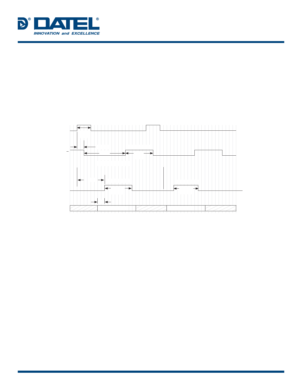
START
CONVERT
INTERNAL S/H
N
20ns
typ.
N+1
12ns typ.
Acquisition Time
Hold
69ns typ.
(66ns min., 72ns max.)
31ns
typ.
DATA
VALID
50ns
DATA N-1 VALID
40ns typ.
(±5ns)
DATA N VALID
40ns typ.
(±5ns)
OUTPUT
DATA
10ns
DATA N-1 VALID
INVALID DATA
DATA N VALID
Notes:
1. Scale is approximately 5ns per division. Sampling rate = 10MHz.
2. The start convert pulse must be between 20 and 50ns wide or between 80 and 100ns wide (when sampling at 10MHz)
to ensure proper operation. For sampling rates less than 10MHz, the start pulse can be wider than 85nsec, however a minimum
pulse width low of 15nsec should be maintained. A 10MHz clock with a 20nsec positive pulse width is used for all production testing.
3. For no latency delay and an input range of ±0.5 Volts, order ADS-947MC-31122.
Figure 4. ADS-947 Timing Diagram
DATEL, Inc. 11 Cabot Boulevard, Mansfield, MA 02048-1151 USA • Tel: (508) 339-3000 • www.datel.com • e-mail: [email protected]
MDA_ADS-947.D01 Page 5 of 9
5 Page | ||
| Páginas | Total 9 Páginas | |
| PDF Descargar | [ Datasheet ADS-947.PDF ] | |
Hoja de datos destacado
| Número de pieza | Descripción | Fabricantes |
| ADS-944 | 5MHz Sampling A/D Converters | DATEL |
| ADS-946 | 8MHz Sampling A/D Converters | Datel |
| ADS-947 | 10MHz Sampling A/D Converters | Datel |
| Número de pieza | Descripción | Fabricantes |
| SLA6805M | High Voltage 3 phase Motor Driver IC. |
Sanken |
| SDC1742 | 12- and 14-Bit Hybrid Synchro / Resolver-to-Digital Converters. |
Analog Devices |
|
DataSheet.es es una pagina web que funciona como un repositorio de manuales o hoja de datos de muchos de los productos más populares, |
| DataSheet.es | 2020 | Privacy Policy | Contacto | Buscar |
