|
|
|
PDF IDT82V2048 Data sheet ( Hoja de datos )
| Número de pieza | IDT82V2048 | |
| Descripción | OCTAL T1/E1 SHORT HAUL LINE INTERFACE UNIT | |
| Fabricantes | IDT | |
| Logotipo | ||
Hay una vista previa y un enlace de descarga de IDT82V2048 (archivo pdf) en la parte inferior de esta página. Total 30 Páginas | ||
|
No Preview Available !
OCTAL T1/E1 SHORT HAUL
LINE INTERFACE UNIT
IDT82V2048
FEATURES
♦ Fully integrated octal T1/E1 short haul line interface which
supports 100Ω T1 twisted pair, 120Ω E1 twisted pair and 75Ω
E1 coaxial applications
♦ Selectable single rail or dual rail mode and AMI or HDB3/B8ZS
line encoder/decoder
♦ Built-in transmit pre-equalization meets G.703 & T1.102
♦ Selectable transmit/receive jitter attenuator meets ETSI CTR12/
13, ITU G.736, G.742,G.823 and AT&T Pub 62411 specifications
♦ SONET/SDH optimized jitter attenuator meets ITU G.783 map-
ping jitter specification
♦ Digital/analog LOS detector meets ITU G.775, ETS 300 233 and
T1.231
♦
♦
♦
♦
♦
♦
♦
♦
♦
♦
ITU G.772 non-intrusive monitoring for in-service testing for
any one of channel1 to channel7
Low impedance transmit drivers with tri-state
Selectable hardware and parallel/serial host interface
Local, remote and inband loopback test functions
Hitless Protection Switching (HPS) for 1 to 1 protection with-
out relays
JTAG boundary scan for board test
3.3V supply with 5V tolerant I/O
Low power consumption
Operating Temperature Range: -40°C to +85°C
Available in 144-pin Thin Quad Flat Pack (TQFP_144_DA) and
160-pin Plastic Ball Grid Array (PBGA) packages
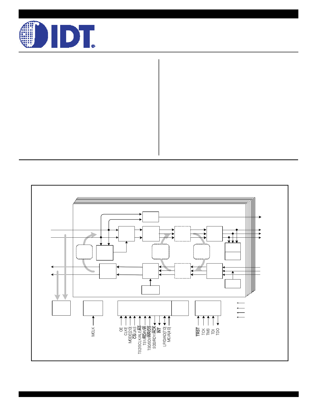
FUNCTIONAL BLOCK DIAGRAM
RTIPn
RRINGn
TTIPn
TRINGn
G.772
Monitor
Analog
Peak
Loopback Detector
Line
Driver
Clock
Generator
Slicer
LOS
Detector
CLK&Data
Recovery
(DPLL)
Digital
Loopback
Waveform
Shaper
Transmit
All Ones
One of Eight Identical Channels
Jitter
Attenuator
B8ZS/
HDB3/AMI
Decoder
Remote
Loopback
IBLC
Detector
AIS
Detector
Jitter
Attenuator
B8ZS/
HDB3/AMI
Encoder
IBLC
Generator
LOSn
RCLKn
RDn/RDPn
CVn/RDNn
TCLKn
TDn/TDPn
BPVIn/TDNn
Control Interface
Register
File
JTAG TAP
VDD IO
VDDT
VDDD
VDDA
Figure - 1. Block Diagram
The IDT logo is a registered trademark of Integrated Device Technology, Inc.
INDUSTRIAL TEMPERATURE RANGES
© 2003 Integrated Device Technology, Inc.
1
DECEMBER 2003
DSC-6037/11
1 page 
IDT82V2048 OCTAL T1/E1 SHORT HAUL LINE INTERFACE UNIT
INDUSTRIAL TEMPERATURE RANGES
PIN DESCRIPTION (CONTINUED)
Name
TD0/TDP0
TD1/TDP1
TD2/TDP2
TD3/TDP3
TD4/TDP4
TD5/TDP5
TD6/TDP6
TD7/TDP7
BPVI0/TDN0
BPVI1/TDN1
BPVI2/TDN2
BPVI3/TDN3
BPVI4/TDN4
BPVI5/TDN5
BPVI6/TDN6
BPVI7/TDN7
Type
Pin No.
QFP144 BGA160
Description
37 N2 TDn: Transmit Data for Channel 0~7
30 L2 When the device is in Single Rail Mode, the NRZ data to be transmitted is input on this pin. Data on
80 L13 TDn is sampled into the device on falling edges of TCLKn, and encoded by AMI or HDB3/B8ZS line
73 N13 code rules before being transmitted to the line.
108 B13
101 D13 BPVIn: Bipolar Violation Insertion for Channel 0~7
8 D2 Bipolar violation insertion is available in Single Rail Mode 2 (see table-1) with AMI enabled. A low-to-
1 B2 high transition on this pin will make the next logic one to be transmitted on TDn the same polarity as the
I previous pulse, and violate the AMI rule. This is for testing.
38 N3
31 L3 TDPn/TDNn: Positive/Negative Transmit Data for Channel 0~7
79 L12 When the device is in Dual Rail Mode, the NRZ data to be transmitted for positive/negative pulse is input
72 N12 on this pin. Data on TDPn/TDNn are active high and sampled on falling edge of TCLKn. The line code in
109 B12 dual rail mode is as the follows :
102 D12
TDPn
TDNn
Output Pulse
7 D3
0 0 Space
144 B3
0 1 Negative Pulse
1 0 Positive Pulse
1 1 Space
TCLK0
TCLK1
TCLK2
TCLK3
TCLK4
TCLK5
TCLK6
TCLK7
Pulling pin TDNn high for more than 16 consecutive TCLK clock cycles will configure the corresponding
channel into single rail mode 1 (see table-1 on Page14).
I 36 N1 TCLKn: Transmit Clock for Channel 0~7
29 L1 The clock of 1.544 MHz (for T1 mode) or 2.048 MHz (for E1 mode) for transmit is input on this pin. The
81 L14 transmit data at TDn/TDPn or TDNn is sampled into the device on falling edge of TCLKn.
74 N14 Pulling TCLKn high for more than 16 MCLK cycles, the corresponding transmitter is set in Transmit All
107 B14 One (TAO) state (when MCLK is clocked). In TAO state, the TAO generator adopts MCLK as the time
100 D14 reference.
9 D1 If TCLKn is Low, the corresponding transmit channel is set into power down state, while driver output
2 B1 ports become high impedance.
Different combinations of TCLKn and MCLK result in different transmit mode. It is summarized as the
follows:
MCLK
TCLKn
Transmitter Mode
Clocked
Clocked
Normal operation
Clocked
High (≥ 16 MCLK) Transmit All One (TAO) signals to the line side in the
corresponding transmit channel.
Clocked Low (≥ 64 MCLK) Corresponding transmit channel is set into power down state.
High/Low TCLK1 is clocked TCLKn is clocked Normal operation
TCLKn is high Transmit All One (TAO) signals to the line side
(≥ 16 TCLK1) in the corresponding transmit channel.
TCLKn is low Corresponding transmit channel is set into
(≥ 64 TCLK1) power down state.
The receive path is not affected by the status of TCLK1. When
MCLK is high, all receive paths just slice the incoming data stream.
When MCLK is low, all the receive paths are powered down.
High/Low
TCLK1 is not All eight transmitters (TTIPn & TRINGn) will be in high impedance
available state.
(High/Low)
5
5 Page 
IDT82V2048 OCTAL T1/E1 SHORT HAUL LINE INTERFACE UNIT
INDUSTRIAL TEMPERATURE RANGES
PIN DESCRIPTION (CONTINUED)
Name
TRST
TMS
TCK
Type
I
Pullup
I
Pullup
I
Pin No.
QFP144 BGA160
Description
JTAG Signals
95 G12 TRST: JTAG Test Port Reset (Active Low)
This is the active low asynchronous reset to the JTAG Test Port. This pin has an internal pullup
resistor and it can be left disconnected.
96 F11 TMS: JTAG Test Mode Select
The signal on this pin controls the JTAG test performance and is clocked into the device on rising
edges of TCK. This pin has an internal pullup resistor and it can be left disconnected.
97 F14 TCK: JTAG Test Clock
This pin input the clock of the JTAG Test. The data on TDI and TMS are clocked into the device on
rising edges of TCK, while the data on TDO is clocked out of the device on falling edges of TCK.
TDO O
98
Tri-state
TDI I 99
Pull up
IC - 93
IC - 94
VDDIO
GNDIO
VDDT0
VDDT1
VDDT2
VDDT3
VDDT4
VDDT5
VDDT6
VDDT7
GNDT0
GNDT1
GNDT2
GNDT3
GNDT4
GNDT5
GNDT6
GNDT7
VDDD
VDDA
GNDD
GNDA
-
-
-
-
-
-
17
92
18
91
44
53
56
65
116
125
128
137
47
50
59
62
119
122
131
134
19
90
20
89
F13 TDO: JTAG Test Data Output
This pin output the serial data of the JTAG Test. The data on TDO is clocked out of the device on
falling edges of TCK. TDO is a Tri-state output signal. It is active only when scanning of data is
out.
F12 TDI: JTAG Test Data Input
This pin input the serial data of the JTAG Test. The data on TDI is clocked into the device on rising
edges of TCK. This pin has an internal pullup resistor and it can be left disconnected.
G13 IC: Internal Connected
(Leave it open for normal operation.)
H13 IC: Internal Connected
(Leave it open for normal operation.)
Supplies and Grounds
G1 3.3V I/O Power Supply
G14
G4 I/O GND
G11
N4,P4 3.3V / 5V Power Supply for Transmitter Driver
L4,M4 All VDDT pins must be connected to either 3.3V or 5V. It is not allowed to leave any of the VDDT
L11,M11 pins open (not-connected) even if the channel is not used.
N11,P11
A11,B11
C11,D11
C4,D4
A4,B4
N6,P6 Analog GND for Transmitter Driver
L6,M6
L9,M9
N9,P9
A9,B9
C9,D9
C6,D6
A6,B6
H1 3.3V Digital / Analog Core Power Supply
H14
H4 Digital / Analog Core GND
H11
11
11 Page | ||
| Páginas | Total 30 Páginas | |
| PDF Descargar | [ Datasheet IDT82V2048.PDF ] | |
Hoja de datos destacado
| Número de pieza | Descripción | Fabricantes |
| IDT82V2041E | SINGLE CHANNEL T1/E1/J1 SHORT HAUL LINE INTERFACE UNIT | IDT |
| IDT82V2044 | QUAD T1/E1 SHORT HAUL LINE INTERFACE UNIT | IDT |
| IDT82V2044E | QUAD CHANNEL T1/E1/J1 SHORT HAUL LINE INTERFACE UNIT | IDT |
| IDT82V2048 | OCTAL T1/E1 SHORT HAUL LINE INTERFACE UNIT | IDT |
| Número de pieza | Descripción | Fabricantes |
| SLA6805M | High Voltage 3 phase Motor Driver IC. |
Sanken |
| SDC1742 | 12- and 14-Bit Hybrid Synchro / Resolver-to-Digital Converters. |
Analog Devices |
|
DataSheet.es es una pagina web que funciona como un repositorio de manuales o hoja de datos de muchos de los productos más populares, |
| DataSheet.es | 2020 | Privacy Policy | Contacto | Buscar |