|
|
|
PDF FDPC5018SG Data sheet ( Hoja de datos )
| Número de pieza | FDPC5018SG | |
| Descripción | MOSFET ( Transistor ) | |
| Fabricantes | Fairchild Semiconductor | |
| Logotipo | ||
Hay una vista previa y un enlace de descarga de FDPC5018SG (archivo pdf) en la parte inferior de esta página. Total 12 Páginas | ||
|
No Preview Available !
FDPC5018SG
PowerTrench® Power Clip
30V Asymmetric Dual N-Channel MOSFET
September 2015
Features
General Description
Q1: N-Channel
Max rDS(on) = 5.0 mΩ at VGS = 10 V, ID = 17 A
Max rDS(on) = 6.5 mΩ at VGS = 4.5 V, ID = 14 A
Q2: N-Channel
Max rDS(on) = 1.6 mΩ at VGS = 10 V, ID = 32 A
Max rDS(on) = 2.0 mΩ at VGS = 4.5 V, ID = 28 A
Low Inductance Packaging Shortens Rise/Fall Times, Result-
ing in Lower Switching Losses
MOSFET Integration Enables Optimum Layout for
Lower Circuit Inductance and Reduced Switch
Node Ringing
This device includes two specialized N-Channel MOSFETs in a
dual package. The switch node has been internally connected to
enable easy placement and routing of synchronous buck
converters. The control MOSFET (Q1) and synchronous
SyncFETTM (Q2) have been designed to provide optimal power
efficiency.
Applications
Computing
Communications
General Purpose Point of Load
RoHS Compliant
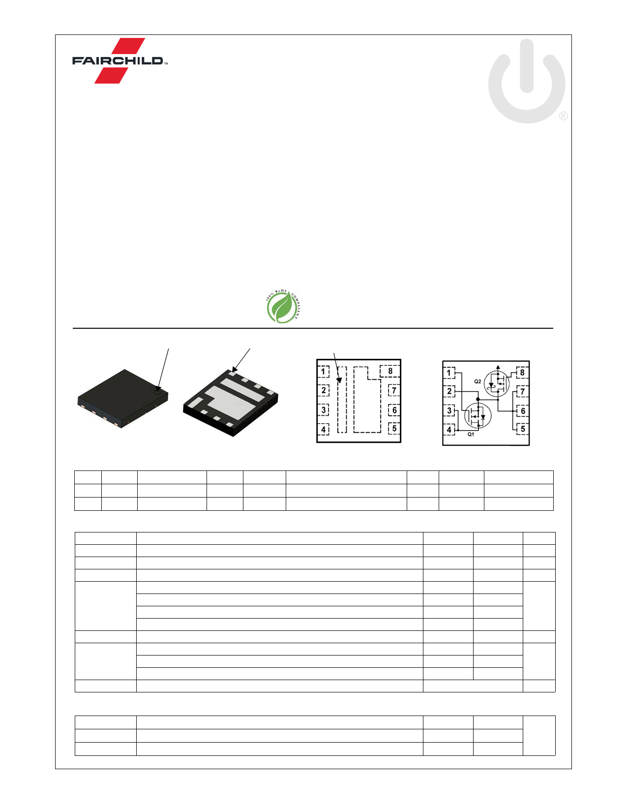
PIN1
PIN1
PAD10
V+(HSD)
HSG
GR
V+
V+
PAD9
GND(LSS)
LSG HSG
SW GR
SW V+
SW V+
SW
LSG
SW
SW
SW
Top Power Clip 5X6 Bottom
Pin Name Description
Pin Name
Description
Pin
1 HSG HighSideGate 3,4,10 V+(HSD) High Side Drain
8
2 GR
Gate Return
5,6,7 SW
Switching Node, Low Side Drain 9
MOSFET Maximum Ratings TA = 25 °C unless otherwise noted.
Name
Description
LSG
Low Side Gate
GND(LSS) Low Side Source
Symbol
VDS
Bvdsst
VGS
ID
EAS
PD
TJ, TSTG
Parameter
Drain to Source Voltage
Bvdsst (transient ) < 100nS
Gate to Source Voltage
Drain Current -Continuous
-Continuous
-Continuous
-Pulsed
Single Pulse Avalanche Energy
Power Dissipation for Single Operation
Power Dissipation for Single Operation
Power Dissipation for Single Operation
Operating and Storage Junction Temperature Range
TC = 25 °C (Note 5)
TC = 100 °C (Note 5)
TA = 25 °C
TA = 25 °C (Note 4)
(Note 3)
TC = 25 °C
TA = 25 °C
TA = 25 °C
Q1 Q2
30 30
32.5 32.5
±20 ±12
56 109
35
17Note1a
69
32Note1b
227 704
54 181
23
2.1Note1a
1.0Note1c
29
2.3Note1b
1.1Note1d
-55 to +150
Units
V
V
V
A
mJ
W
°C
Thermal Characteristics
RθJC
RθJA
RθJA
Thermal Resistance, Junction to Case
Thermal Resistance, Junction to Ambient
Thermal Resistance, Junction to Ambient
5.6
60Note1a
130Note1c
4.3
55Note1b
120Note1d
°C/W
©2015 Fairchild Semiconductor Corporation
FDPC5018SG Rev.1.1
1
www.fairchildsemi.com
1 page 
Typical Characteristics (Q1 N-Channel) TJ = 25°C unless otherwise noted.
10
ID = 17 A
8
VDD = 10 V
6
VDD = 15 V
4
VDD = 20 V
2
0
0 4 8 12 16
Qg, GATE CHARGE (nC)
20
3000
1000
Ciss
Coss
100 Crss
f = 1 MHz
VGS = 0 V
10
0.1
1
10
VDS, DRAIN TO SOURCE VOLTAGE (V)
30
Figure 7. Gate Charge Characteristics
Figure8. Capacitancevs.Drain
to Source Voltage
30 60
10
TJ = 25 oC
TJ = 125 oC
1
0.001
0.01 0.1
1
10
tAV, TIME IN AVALANCHE (ms)
100
Figure9. UnclampedInductive
Switching Capability
500
100
10 μs
10
THIS AREA IS
LIMITED BY rDS(on)
1
SINGLE PULSE
TJ = MAX RATED
RθJC = 5.6 oC/W
TC = 25 oC
0.1
0.1 1
CURVE BENT TO
MEASURED DATA
10
100 μs
1 ms
10 ms
DC
80
VDS, DRAIN to SOURCE VOLTAGE (V)
Figure 11. Forward Bias Safe
Operating Area
45
VGS = 10 V
30
VGS = 4.5 V
15
RθJC = 5.6 oC/W
0
25 50 75 100 125
TC, CASE TEMPERATURE (oC)
150
Figure 10. Maximum Continuous Drain
Current vs. Case Temperature
5000
1000
SINGLE PULSE
RθJC = 5.6 oC/W
TC = 25 oC
100
10
10-5
10-4
10-3
10-2
t, PULSE WIDTH (sec)
10-1
Figure 12. Single Pulse Maximum
Power Dissipation
1
©2015 Fairchild Semiconductor Corporation
FDPC5018SG Rev.1.1
5
www.fairchildsemi.com
5 Page 
0.10 C
2X
4
5.10
4.90
PKG
CL
1
PKG CL
PIN #1 5
8
INDICATOR
TOP VIEW
A
B
5.00
4.56
4.20
1.27
43 2
1
1.01
3.30
2.48
2.08
6.10
5.90
0.10 C
2X
6.60
0.00
2.65
0.82
5 6 78
0.75
0.40
0.83
1.43
1.98
2.48
3.30
SEE
DETAIL A
RECOMMENDED LAND PATTERN
SIDE VIEW
3.15±.05
3.81
1.27
56 7 8
0.10 C A B
0.05 C
0.51
0.65±.05
2.46±.05
0.91±.05
0.49±.05
4 32
1
0.51±.05
3.90±.05
4.22±.05
5.00±.05
BOTTOM VIEW
1.57±.05
0.65±.05
1.37±.05
0.53±.05
0.48±.05
NOTES: UNLESS OTHERWISE SPECIFIED
A) DOES NOT FULLY CONFORM TO
JEDEC REGISTRATION, MO-229,
DATED 11/2001.
B) ALL DIMENSIONS ARE IN
MILLIMETERS.
C) DIMENSIONS DO NOT INCLUDE
BURRS OR MOLD FLASH. MOLD
FLASH OR BURRS DOES NOT
EXCEED 0.10MM.
D) DIMENSIONING AND TOLERANCING
PER ASME Y14.5M-1994.
E) DRAWING FILE NAME: PQFN08KREV2
0.10 C
0.08 C
0.80
0.70
0.30
0.20
0.05
0.00
(SCALE: 2X)
C
SEATING
PLANE
11 Page | ||
| Páginas | Total 12 Páginas | |
| PDF Descargar | [ Datasheet FDPC5018SG.PDF ] | |
Hoja de datos destacado
| Número de pieza | Descripción | Fabricantes |
| FDPC5018SG | MOSFET ( Transistor ) | Fairchild Semiconductor |
| Número de pieza | Descripción | Fabricantes |
| SLA6805M | High Voltage 3 phase Motor Driver IC. |
Sanken |
| SDC1742 | 12- and 14-Bit Hybrid Synchro / Resolver-to-Digital Converters. |
Analog Devices |
|
DataSheet.es es una pagina web que funciona como un repositorio de manuales o hoja de datos de muchos de los productos más populares, |
| DataSheet.es | 2020 | Privacy Policy | Contacto | Buscar |