|
|
|
PDF FDMC8321LDC Data sheet ( Hoja de datos )
| Número de pieza | FDMC8321LDC | |
| Descripción | MOSFET ( Transistor ) | |
| Fabricantes | Fairchild Semiconductor | |
| Logotipo | ||
Hay una vista previa y un enlace de descarga de FDMC8321LDC (archivo pdf) en la parte inferior de esta página. Total 8 Páginas | ||
|
No Preview Available !
December 2014
FDMC8321LDC
N-Channel Power Trench® MOSFET
40 V, 108 A, 2.5 mΩ
Features
Dual CoolTM Top Side Cooling PQFN package
Max rDS(on) = 2.5 mΩ at VGS = 10 V, ID = 27 A
Max rDS(on) = 4.1 mΩ at VGS = 4.5 V, ID = 21 A
High performance technology for extremely low rDS(on)
RoHS Compliant
General Description
This N-Channel MOSFET is produced using Fairchild
Semiconductor’s advanced PowerTrench® process.
Advancements in both silicon and Dual CoolTM package
technologies have been combined to offer the lowest rDS(on)
while maintaining excellent switching performance by extremely
low Junction-to-Ambient thermal resistance.
Applications
Primary DC-DC Switch
Motor Bridge Switch
Synchronous Rectifier
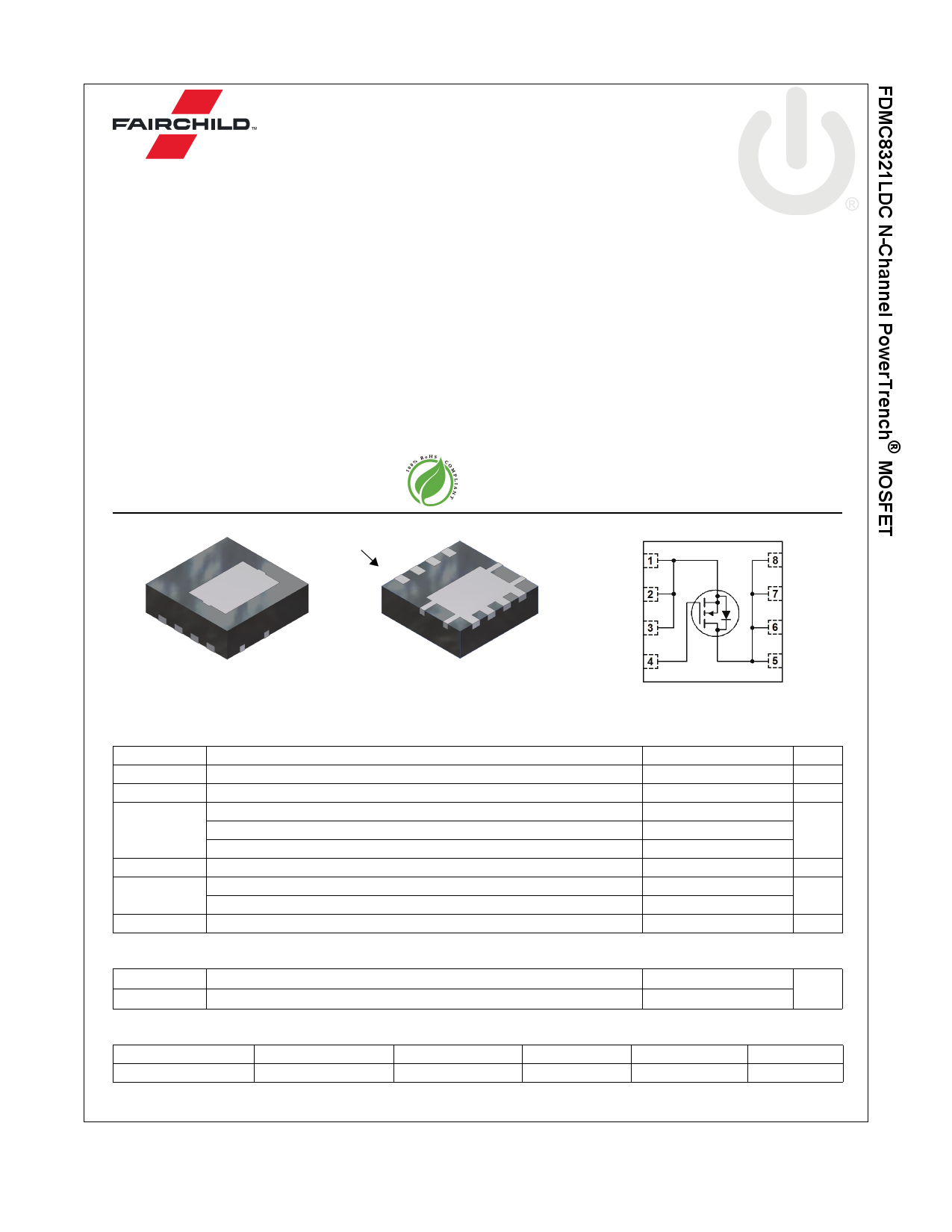
Pin 1
G
S
S
S
Top Power 33
D DDD
Bottom
S
S
S
G
D
D
D
D
MOSFET Maximum Ratings TA = 25 °C unless otherwise noted
Symbol
VDS
VGS
ID
Parameter
Drain to Source Voltage
Gate to Source Voltage
Drain Current
-Continuous
-Continuous
-Pulsed
TC = 25 °C
TA = 25 °C
EAS
PD
TJ, TSTG
Single Pulse Avalanche Energy
Power Dissipation
TC = 25 °C
Power Dissipation
TA = 25 °C
Operating and Storage Junction Temperature Range
Thermal Characteristics
(Note 1a)
(Note 4)
(Note 3)
(Note 1a)
Ratings
40
±20
108
27
320
181
56
2.9
-55 to +150
Units
V
V
A
mJ
W
°C
RθJC
RθJA
Thermal Resistance, Junction to Case
Thermal Resistance, Junction to Ambient
Package Marking and Ordering Information
(Note 1)
(Note 1a)
2.2
42
°C/W
Device Marking
8321LD
Device
FDMC8321LDC
Package
Power33
Reel Size
13 ’’
Tape Width
12 mm
Quantity
3000 units
©2014 Fairchild Semiconductor Corporation
FDMC8321LDC Rev.C
1
www.fairchildsemi.com
1 page 
Typical Characteristics TJ = 25 °C unless otherwise noted
10
ID = 27 A
8
6
4
VDD = 16 V
VDD = 20 V
VDD = 24 V
2
0
0 10 20 30 40
Qg, GATE CHARGE (nC)
50
10000
1000
Ciss
Coss
100
Crss
f = 1 MHz
VGS = 0 V
10
0.1 1 10
VDS, DRAIN TO SOURCE VOLTAGE (V)
40
Figure 7. Gate Charge Characteristics
Figure8. CapacitancevsDrain
to Source Voltage
100
10 TJ = 25 oC
TJ = 100 oC
1
0.01
TJ = 125 oC
0.1 1 10
tAV, TIME IN AVALANCHE (ms)
Figure9. UnclampedInductive
Switching Capability
100
120
RθJC = 2.2 oC/W
100
80
60
Limited by Package
40
VGS = 10 V
VGS = 4.5 V
20
0
25 50 75 100 125 150
TC, CASE TEMPERATURE (oC)
Figure 10. Maximum Continuous Drain
Current vs Case Temperature
600
100
10 us
10
THIS AREA IS
LIMITED BY rDS(on)
1
SINGLE PULSE
TJ = MAX RATED
RθJC = 2.2 oC/W
TC = 25 oC
0.1
0.1
1
CURVE BENT TO
MEASURED DATA
10
VDS, DRAIN to SOURCE VOLTAGE (V)
100 us
1 ms
10 ms
DC
100
Figure 11. Forward Bias Safe
Operating Area
10000
1000
SINGLE PULSE
RθJC = 2.2 oC/W
TC = 25 oC
100
10
10-5
10-4
10-3
10-2
t, PULSE WIDTH (sec)
10-1
Figure 12. Single Pulse Maximum
Power Dissipation
1
©2014 Fairchild Semiconductor Corporation
FDMC8321LDC Rev.C
5
www.fairchildsemi.com
5 Page | ||
| Páginas | Total 8 Páginas | |
| PDF Descargar | [ Datasheet FDMC8321LDC.PDF ] | |
Hoja de datos destacado
| Número de pieza | Descripción | Fabricantes |
| FDMC8321LDC | MOSFET ( Transistor ) | Fairchild Semiconductor |
| Número de pieza | Descripción | Fabricantes |
| SLA6805M | High Voltage 3 phase Motor Driver IC. |
Sanken |
| SDC1742 | 12- and 14-Bit Hybrid Synchro / Resolver-to-Digital Converters. |
Analog Devices |
|
DataSheet.es es una pagina web que funciona como un repositorio de manuales o hoja de datos de muchos de los productos más populares, |
| DataSheet.es | 2020 | Privacy Policy | Contacto | Buscar |