|
|
|
PDF FDMD85100 Data sheet ( Hoja de datos )
| Número de pieza | FDMD85100 | |
| Descripción | MOSFET ( Transistor ) | |
| Fabricantes | Fairchild Semiconductor | |
| Logotipo | ||
Hay una vista previa y un enlace de descarga de FDMD85100 (archivo pdf) en la parte inferior de esta página. Total 11 Páginas | ||
|
No Preview Available !
September 2015
FDMD85100
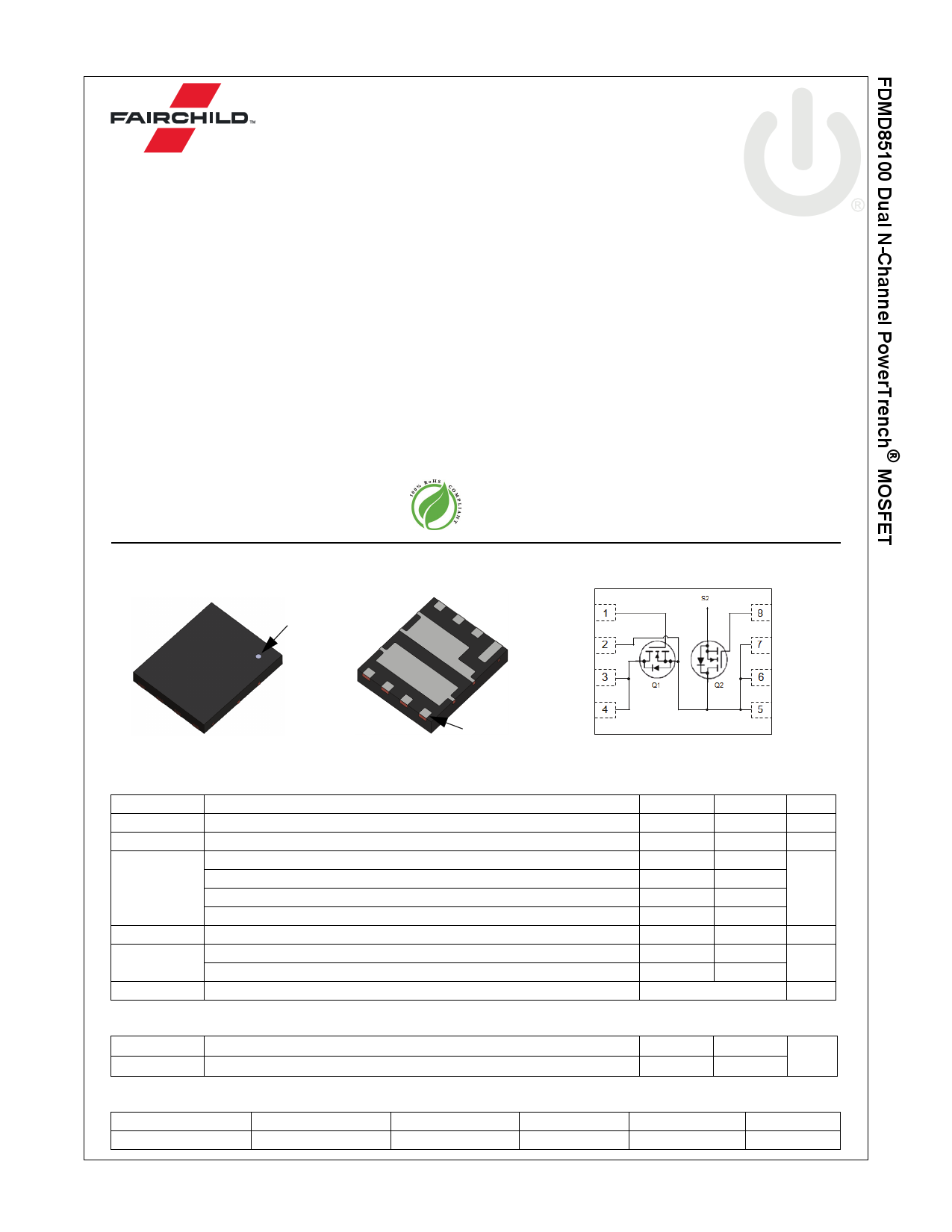
Dual N-Channel PowerTrench® MOSFET
Q1: 100 V, 48A, 9.9 mΩ Q2: 100 V, 48A, 9.9 mΩ
Features
General Description
Q1: N-Channel
Max rDS(on) = 9.9 mΩ at VGS = 10 V, ID = 10.4 A
Max rDS(on) = 16.4 mΩ at VGS = 6 V, ID = 8 A
Q2: N-Channel
Max rDS(on) = 9.9 mΩ at VGS = 10 V, ID = 10.4 A
Max rDS(on) = 16.4 mΩ at VGS = 6 V, ID = 8 A
Ideal for flexible layout in primary side of bridge topology
Termination is Lead-free and RoHS Compliant
100% UIL tested
Kelvin High Side MOSFET drive pin-out capability
This device includes two 100V N-Channel MOSFETs in a dual
Power (5 mm X 6 mm) package. HS source and LS Drain
internally connected for half/full bridge, low source inductance
package, low rDS(on)/Qg FOM silicon.
Applications
Synchronous Buck : Primary Switch of Half / Full Bridge
Bonverter for Telecom
Motor Bridge : Primary Switch of Half / Full Bridge Converter
for BLDC Motor
MV POL : 48V Synchronous Buck Switch
Half/Full Bridge Secondary Synchronous Rectification
Top Bottom
Pin 1
D2/S1
D2/S1
D2/S1
S2 G2
G1
GR
G2
D2/S1
D1 D1
D1
GR
G1
Pin 1
Power 5 x 6
MOSFET Maximum Ratings TA = 25 °C unless otherwise noted.
Symbol
VDS
VGS
ID
Drain to Source Voltage
Gate to Source Voltage
Drain Current -Continuous
-Continuous
Drain Current -Continuous
-Pulsed
Parameter
TC = 25 °C
TC = 100 °C
TA = 25 °C
EAS
PD
TJ, TSTG
Single Pulse Avalanche Energy
Power Dissipation
TC = 25 °C
Power Dissipation
TA = 25 °C
Operating and Storage Junction Temperature Range
Thermal Characteristics
D1
D1
(Note 5)
(Note 5)
(Note 4)
(Note 3)
D2/S1
D2/S1
Q1 Q2
100 100
±20 ±20
48 48
30
10.41a
30
10.41b
261 261
294 294
50
2.21a
50
2.21b
-55 to +150
Units
V
V
A
mJ
W
°C
RθJC
RθJA
Thermal Resistance, Junction-to-Case
Thermal Resistance, Junction-to-Ambient
Package Marking and Ordering Information
2.5
551a
2.5
55 1b
°C/W
Device Marking
FDMD85100
Device
FDMD85100
Package
Power 5 x 6
Reel Size
13 ’’
Tape Width
12 mm
Quantity
3000 units
©2015 Fairchild Semiconductor Corporation
FDMD85100 Rev.1.2
1
www.fairchildsemi.com
1 page 
Typical Characteristics (Q1 N-Channel) TJ = 25°C unless otherwise noted.
10
ID = 10.4 A
8
6
4
VDD = 25 V
VDD = 50 V
VDD = 75 V
2
0
0 4 8 12 16 20 24
Qg, GATE CHARGE (nC)
10000
1000
Ciss
Coss
100
Crss
10
f = 1 MHz
VGS = 0 V
5
0.1
1
10
VDS, DRAIN TO SOURCE VOLTAGE (V)
100
Figure 7. Gate Charge Characteristics
Figure8. Capacitancevs.Drain
to Source Voltage
100
TJ = 25 oC
10 TJ = 100 oC
TJ = 125 oC
1
0.001
0.01 0.1 1 10
tAV, TIME IN AVALANCHE (ms)
Figure9. UnclampedInductive
Switching Capability
100
50
RθJC = 2.5 oC/W
40
VGS = 10 V
30
VGS = 6 V
20
10
0
25 50 75 100 125 150
TC, CASE TEMPERATURE (oC)
Figure 10. Maximum Continuous Drain
Current vs. Case Temperature
1000
100
10 μs
10
THIS AREA IS
1 LIMITED BY rDS(on)
SINGLE PULSE
0.1
TJ = MAX RATED
RθJC = 2.5 oC/W
TC = 25 oC
0.01
0.1
1
CURVE BENT TO
MEASURED DATA
10
100 μs
1 ms
10 ms
DC
100 400
VDS, DRAIN to SOURCE VOLTAGE (V)
Figure 11. Forward Bias Safe
Operating Area
10000
1000
SINGLE PULSE
RθJC = 2.5 oC/W
TC = 25 oC
100
10
10-5
10-4
10-3
10-2
t, PULSE WIDTH (sec)
10-1
1
Figure 12. Single Pulse Maximum Power
Dissipation
©2015 Fairchild Semiconductor Corporation
FDMD85100 Rev.1.2
5
www.fairchildsemi.com
5 Page 
ON Semiconductor and are trademarks of Semiconductor Components Industries, LLC dba ON Semiconductor or its subsidiaries in the United States and/or other countries.
ON Semiconductor owns the rights to a number of patents, trademarks, copyrights, trade secrets, and other intellectual property. A listing of ON Semiconductor’s product/patent
coverage may be accessed at www.onsemi.com/site/pdf/Patent−Marking.pdf. ON Semiconductor reserves the right to make changes without further notice to any products herein.
ON Semiconductor makes no warranty, representation or guarantee regarding the suitability of its products for any particular purpose, nor does ON Semiconductor assume any liability
arising out of the application or use of any product or circuit, and specifically disclaims any and all liability, including without limitation special, consequential or incidental damages.
Buyer is responsible for its products and applications using ON Semiconductor products, including compliance with all laws, regulations and safety requirements or standards,
regardless of any support or applications information provided by ON Semiconductor. “Typical” parameters which may be provided in ON Semiconductor data sheets and/or
specifications can and do vary in different applications and actual performance may vary over time. All operating parameters, including “Typicals” must be validated for each customer
application by customer’s technical experts. ON Semiconductor does not convey any license under its patent rights nor the rights of others. ON Semiconductor products are not
designed, intended, or authorized for use as a critical component in life support systems or any FDA Class 3 medical devices or medical devices with a same or similar classification
in a foreign jurisdiction or any devices intended for implantation in the human body. Should Buyer purchase or use ON Semiconductor products for any such unintended or unauthorized
application, Buyer shall indemnify and hold ON Semiconductor and its officers, employees, subsidiaries, affiliates, and distributors harmless against all claims, costs, damages, and
expenses, and reasonable attorney fees arising out of, directly or indirectly, any claim of personal injury or death associated with such unintended or unauthorized use, even if such
claim alleges that ON Semiconductor was negligent regarding the design or manufacture of the part. ON Semiconductor is an Equal Opportunity/Affirmative Action Employer. This
literature is subject to all applicable copyright laws and is not for resale in any manner.
PUBLICATION ORDERING INFORMATION
LITERATURE FULFILLMENT:
Literature Distribution Center for ON Semiconductor
19521 E. 32nd Pkwy, Aurora, Colorado 80011 USA
Phone: 303−675−2175 or 800−344−3860 Toll Free USA/Canada
Fax: 303−675−2176 or 800−344−3867 Toll Free USA/Canada
Email: [email protected]
© Semiconductor Components Industries, LLC
N. American Technical Support: 800−282−9855 Toll Free
USA/Canada
Europe, Middle East and Africa Technical Support:
Phone: 421 33 790 2910
Japan Customer Focus Center
Phone: 81−3−5817−1050
www.onsemi.com
1
ON Semiconductor Website: www.onsemi.com
Order Literature: http://www.onsemi.com/orderlit
For additional information, please contact your local
Sales Representative
www.onsemi.com
11 Page | ||
| Páginas | Total 11 Páginas | |
| PDF Descargar | [ Datasheet FDMD85100.PDF ] | |
Hoja de datos destacado
| Número de pieza | Descripción | Fabricantes |
| FDMD85100 | MOSFET ( Transistor ) | Fairchild Semiconductor |
| Número de pieza | Descripción | Fabricantes |
| SLA6805M | High Voltage 3 phase Motor Driver IC. |
Sanken |
| SDC1742 | 12- and 14-Bit Hybrid Synchro / Resolver-to-Digital Converters. |
Analog Devices |
|
DataSheet.es es una pagina web que funciona como un repositorio de manuales o hoja de datos de muchos de los productos más populares, |
| DataSheet.es | 2020 | Privacy Policy | Contacto | Buscar |