|
|
|
PDF AD9578 Data sheet ( Hoja de datos )
| Número de pieza | AD9578 | |
| Descripción | Dual PLL Precision Synthesizer | |
| Fabricantes | Analog Devices | |
| Logotipo | ||
Hay una vista previa y un enlace de descarga de AD9578 (archivo pdf) en la parte inferior de esta página. Total 30 Páginas | ||
|
No Preview Available !
Data Sheet
Dual PLL Precision Synthesizer
AD9578
FEATURES
Any output frequency precision synthesis
11.8 MHz to 919 MHz
Better than 0.1 ppb frequency resolution
Ultralow rms jitter (12 kHz to 20 MHz)
<300 fs rms using integer synthesis
<405 fs rms using fractional synthesis
Dual reference inputs support LVPECL, LVDS, 1.8 V LVCMOS,
or fundamental mode AT cut crystals from 22 MHz to
54 MHz or reference clocks from 20 MHz to 60 MHz
Numerical (NCO) frequency control
Dynamically pullable output frequency enables FPGA-
based PLLs (HDL available)
Fast serial peripheral interface (SPI) bus write speeds up to
100 MHz
On-the-fly frequency changes
Dual PLL in compact 7 mm × 7 mm package
Replaces multiple large clock ICs, PLLs, fanout buffers,
crystal oscillators (XOs), and voltage controlled crystal
oscillators (VCXOs)
Mix and match output buffers
In-circuit programmable LVPECL/LVDS/HCSL/LVCMOS
Independent buffer (VDDOx) drives multiple technologies
Enhanced power supply noise rejection
APPLICATIONS
FPGA-based jitter attenuators and low jitter PLLs
Precision disciplined clocks and clock synthesizers
Multirate clock synthesizers
Optical: OTN/SDH/SONET
Broadcast video: 3G SDI, HD SDI, SDI
Networking and storage: Ethernet/SAS/Fibre Channel
Wireless infrastructure: OBSAI/CPRI
Industrial: IEEE 1588
Numerically controlled oscillators (NCOs)
GENERAL DESCRIPTION
The AD9578 is a programmable synthesizer intended for jitter
attenuation and asynchronous clocking applications in high
performance telecommunications, networking, data storage,
serializer/deserializer (SERDES), and physical layer (PHY)
applications. The device incorporates two low jitter PLLs that
provide any frequency with precision better than 0.1 ppb, each
with two separate output dividers, for a total of four programmable
outputs, delivering maximum flexibility and jitter performance.
Each output is independently programmable to provide frequen-
cies of up to 919 MHz with <410 fs typical rms jitter (12 kHz to
20 MHz) utilizing compact, low cost fundamental mode crystals
(XTALs) that enable a robust supply chain. Using integer
frequency synthesis, the AD9578 is capable of achieving rms
jitter as low as 290 fs.
The AD9578 is packaged with a factory programmed default
power-on configuration. After power-on, all settings including
output frequency are reconfigurable through a fast SPI.
The AD9578 architecture permits it to be used as a numerically
controlled oscillator (NCO). This allows the user to dynamically
change the frequency using the fast SPI bus. FPGAs and other
devices can take advantage of this function to implement digital
PLLs with configurable loop bandwidths for jitter attenuation
applications, precision disciplined clocks that lock to tight
stability references, or digitally controlled precision timing
applications, such as network timing and IEEE 1588 applications.
The SPI bus can operate up to 50 MHz, enabling fast FPGA
loops while multiple devices share the same bus. The AD9578
can also be used in multirate precision applications, such as
broadcast video or OTN. HDL FPGA code for digital PLL
applications is available from Analog Devices, Inc.
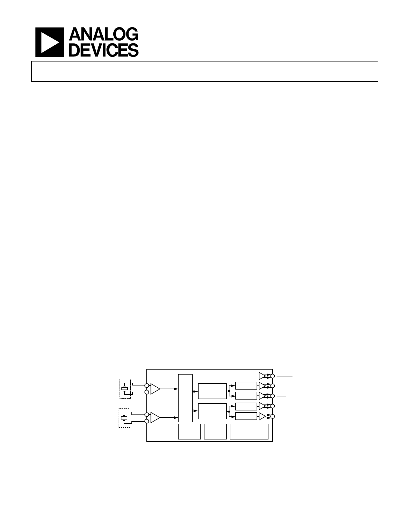
SIMPLIFIED FUNCTIONAL BLOCK DIAGRAM
OPTIONAL
XO4
XO3
OPTIONAL
XO2
XO1
AD9578
REF2
REF1
REF
INPUT
MUX
FRACTIONAL
PLL1
FRACTIONAL
PLL2
DIVIDER
DIVIDER
DIVIDER
DIVIDER
POWER
SUPPLIES
OUTPUT
ENABLE
LOGIC
SPI AND OTP
PROGRAMMABLE
LOGIC CONTROL
REFOUT,
REFOUT
OUT1,
OUT1
OUT2,
OUT2
OUT3,
OUT3
OUT4,
OUT4
NOTES
1. IF SUPPLYING A SINGLE-ENDED 1.8V CMOS SIGNAL, CONNECT THE SIGNAL TO EITHER
XO2 OR XO4.
Figure 1.
Rev. A
Document Feedback
Information furnished by Analog Devices is believed to be accurate and reliable. However, no
responsibility is assumed by Analog Devices for its use, nor for any infringements of patents or other
rights of third parties that may result from its use. Specifications subject to change without notice. No
license is granted by implication or otherwise under any patent or patent rights of Analog Devices.
Trademarksandregisteredtrademarksarethepropertyoftheirrespectiveowners.
One Technology Way, P.O. Box 9106, Norwood, MA 02062-9106, U.S.A.
Tel: 781.329.4700 ©2014–2016 Analog Devices, Inc. All rights reserved.
Technical Support
www.analog.com
1 page 
AD9578
Data Sheet
SPECIFICATIONS
SUPPLY VOLTAGE AND CURRENT (2.5 V OPERATION)
VDD = 2.5 V ± 5%, TA = −25°C to +85°C.
Table 1.
Parameter
SUPPLY VOLTAGE
SUPPLY CURRENT
Symbol
VDD
IDD
Min
Typ Max
Unit
2.375 2.50 2.625 V
229 247 265 mA
337 365 388 mA
Test Conditions/Comments
Using typical configuration in Table 3
Using all blocks running configuration in Table 3
SUPPLY VOLTAGE AND CURRENT (3.3 V OPERATION)
VDD = 3.3 V ± 10%, TA = −25°C to +85°C.
Table 2.
Parameter
Symbol Min Typ Max
Unit Test Conditions/Comments
SUPPLY VOLTAGE VDD
2.97 3.30 3.63
V
VPROG
5.25 5.5 VDD + 2.5 V
CS pin only; used only for one time programmable (OTP) programming;
perform OTP programming only with VDD = 3.3 V
SUPPLY CURRENT IDD
252 268
mA Using typical configuration in Table 3
373 397
mA Using all blocks running configuration in Table 3
POWER DISSIPATION
VDD = 2.5 V ± 5%, TA = −25°C to +85°C. Maximum power is at VDD = 2.625 V and is usually 11% higher than typical.
Table 3.
Parameter
POWER DISSIPATION
Typical Configuration
All Blocks Running
Full Power-Down
Incremental Power Dissipation
Crystal Reference On/Off
PLL On/Off
Output Distribution Driver On/Off
HCSL (at 644.53 MHz)
LVDS (at 644.53 MHz)
LVPECL (at 644.53 MHz)
3.3 V LVCMOS (at 25 MHz)
Min Typ Max Unit Test Conditions/Comments
618 696 mW XTAL: 25 MHz
REFOUT driver: disabled
PLL1: one LVPECL driver at 644.53125 MHz
PLL2: one single-ended LVCMOS driver (with 80 pF load)
at 100 MHz
913 1018 mW XTAL: 49.152 MHz XTAL on both XTAL inputs
REFOUT driver: LVPECL mode, 49.152 MHz
PLL1: two LVPECL drivers at 693.812 MHz
PLL2: two LVPECL drivers at 693.812 MHz
67 75
mW PD1 pin grounded; Register 0x02 = 0x015555 to disable
remainder of chip
Starting with typical configuration; change in power due
to the indicated operation
25 mW
259 mW PLL1 or PLL2 on/off, including output drivers or channel
dividers
75 mW Each output of a differential pair has 50 Ω to ground
43 mW 100 Ω across differential pair
107 mW 50 Ω to VDD – 2 V
75 mW A single 3.3 V LVCMOS output with an 80 pF load
Rev. A | Page 4 of 44
5 Page 
AD9578
DIGITAL PLL
Table 8.
Parameter
FREQUENCY STEP SIZE
Min Typ Max Unit Test Conditions/Comments
0.1 ppb
Data Sheet
DIGITAL FUNCTIONS TIMING
Table 9.
Parameter
Min Typ Max Unit Test Conditions/Comments
OTP PROGRAMMING TIME, PER BIT 0.8
POWER-ON RESET TIME
4
1
2
ms See Table 4 for using CS while in OTP programming mode (the AD9578
has 444 bits; therefore, the total programming time is <1 sec)
ms Do not access serial port during power-on reset.
JITTER GENERATION USING 49.152 MHZ CRYSTAL
Both PLLs are generating the same output frequency and use a 49.152 MHz crystal for the input reference. The loop bandwidth is set to
the default value of 300 kHz. Where multiple driver types are listed, there is no significant difference between driver types.
Table 10.
Parameter
JITTER GENERATION
LVPECL, HCSL, LVDS Driver
fOUT = 622.08 MHz
Bandwidth: 12 kHz to 20 MHz
Bandwidth: 20 kHz to 80 MHz
fOUT = 693.48 MHz
Bandwidth: 12 kHz to 20 MHz
Bandwidth: 20 kHz to 80 MHz
fOUT = 174.703 MHz
Bandwidth: 12 kHz to 20 MHz
Bandwidth: 20 kHz to 80 MHz
fOUT = 161.1328 MHz
Bandwidth: 12 kHz to 20 MHz
Bandwidth: 20 kHz to 80 MHz
LVPECL, HCSL, LVDS, LVCMOS Driver
fOUT = 156.25 MHz
Bandwidth: 12 kHz to 20 MHz
Bandwidth: 1.875 MHz to 20 MHz
Bandwidth: 20 kHz to 80 MHz
Min Typ Max Unit
Test Conditions/Comments
Fractional mode on, fREF = 49.152 MHz XTAL
320 fs rms
370 fs rms
403 fs rms
408 fs rms
403 fs rms
410 fs rms
361 fs rms
363 fs rms
350 fs rms
77 fs rms
352 fs rms
Rev. A | Page 10 of 44
11 Page | ||
| Páginas | Total 30 Páginas | |
| PDF Descargar | [ Datasheet AD9578.PDF ] | |
Hoja de datos destacado
| Número de pieza | Descripción | Fabricantes |
| AD9571 | Ethernet Clock Generator | Analog Devices |
| AD9572 | Fiber Channel/Ethernet Clock Generator IC | Analog Devices |
| AD9573 | PCI-Express Clock Generator IC | Analog Devices |
| AD9574 | Ethernet/Gigabit Ethernet Clock Generator | Analog Devices |
| Número de pieza | Descripción | Fabricantes |
| SLA6805M | High Voltage 3 phase Motor Driver IC. |
Sanken |
| SDC1742 | 12- and 14-Bit Hybrid Synchro / Resolver-to-Digital Converters. |
Analog Devices |
|
DataSheet.es es una pagina web que funciona como un repositorio de manuales o hoja de datos de muchos de los productos más populares, |
| DataSheet.es | 2020 | Privacy Policy | Contacto | Buscar |