|
|
|
PDF AD9877 Data sheet ( Hoja de datos )
| Número de pieza | AD9877 | |
| Descripción | Cable Modem | |
| Fabricantes | Analog Devices | |
| Logotipo | ||
Hay una vista previa y un enlace de descarga de AD9877 (archivo pdf) en la parte inferior de esta página. Total 30 Páginas | ||
|
No Preview Available !
FEATURES
Low cost 3.3 V CMOS MxFE™ for
MCNS-DOCSIS-, DVB-, DAVIC-compliant
set-top box and cable modem applications
232 MHz quadrature digital upconverter
12-bit direct IF DAC (TxDAC+®)
Up to 65 MHz carrier frequency DDS
Programmable sampling clock rates
Selectable interpolation filter
Analog Tx output level adjust
12-bit, 33 MSPS direct IF ADC
Dual 8-bit, 16.5 MSPS sampling IQ ADCs
Two 12-bit Σ-Δ auxiliary DACs
Direct interface to AD8321/AD8325 or
AD8322/AD8327 PGA cable driver
APPLICATIONS
Cable modems
Set-top boxes
Wireless modems
GENERAL DESCRIPTION
The AD9877 is a single-supply set-top box and cable modem
mixed-signal front end. The device contains a transmit path
interpolation filter, complete quadrature digital upconverter,
and transmit DAC. The receive path contains a 12-bit ADC and
dual 8-bit ADCs. All internally required clocks and an output
system clock are generated by the phase-locked loop (PLL) from
a single crystal or clock input.
The transmit path interpolation filter provides upsampling
factors of 12× or 16× with an output signal bandwidth as high
as 5.8 MHz. Carrier frequencies up to 65 MHz with 26 bits of
frequency tuning resolution can be generated by the direct
digital synthesizer (DDS). The transmit DAC resolution is 12 bits
and can run at sampling rates as high as 232 MSPS. Analog
output scaling from 0 dB to 7.5 dB in 0.5 dB steps is available to
preserve SNR when reduced output levels are required.
Mixed-Signal Front End
Set-Top Box, Cable Modem
AD9877
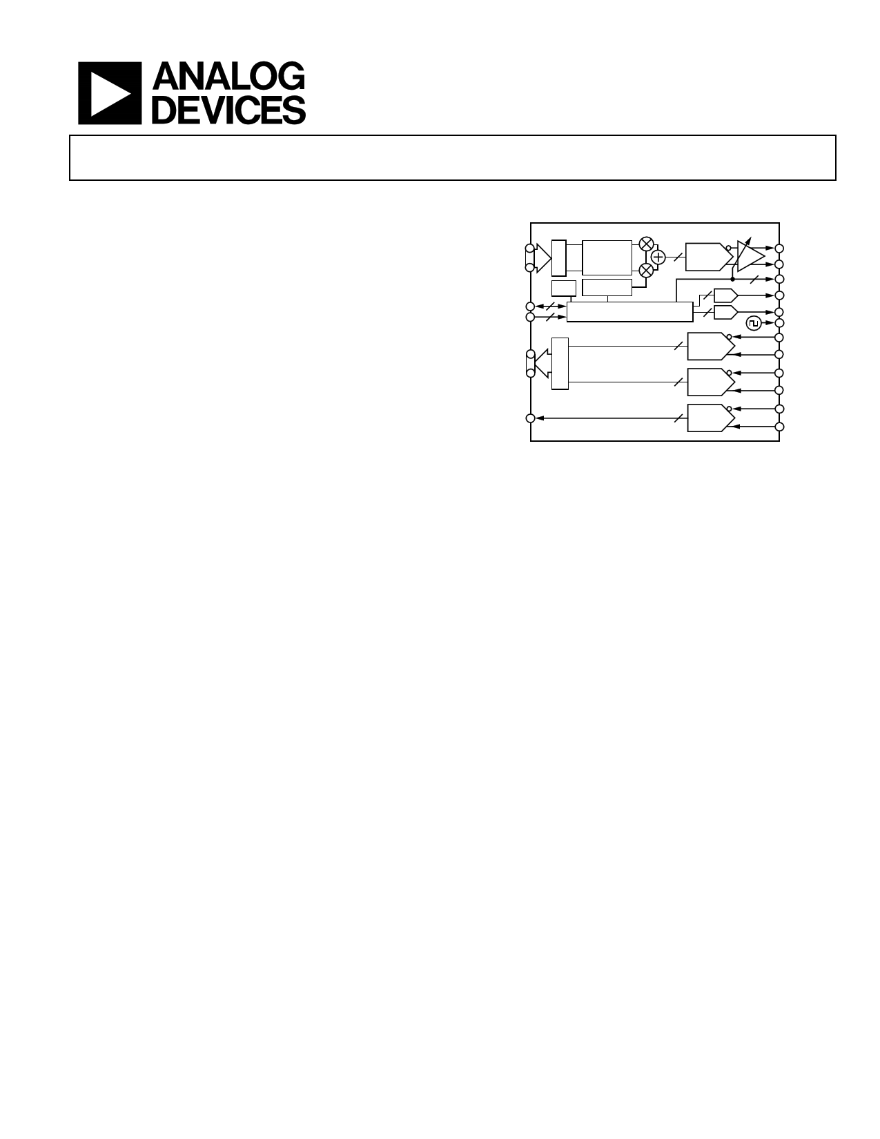
FUNCTIONAL BLOCK DIAGRAM
Tx DATA
SPORT
PROFILE
RxIQ DATA
Tx
PLL
4
2
INTER-
POLATOR
FILTER
DDS
COS
12
SIN
CONTROL FUNCTIONS
8
Rx
8
DAC
12
Σ-Δ
12
Σ-Δ
ADC
ADC
3
Tx
CA
SDELTA0
SDELTA1
REFCLK
I IN
Q IN
RxIF DATA
AD9877
12
ADC
IF IN
Figure 1.
The 12-bit ADC has excellent undersampling performance,
allowing it to typically deliver better than 10 ENOBs with IF
inputs up to 70 MHz. The 12-bit IF ADC can sample at a rate
up to 33 MHz, allowing it to process wideband signal inputs.
Two programmable Σ-Δ DACs are available and can be used to
control external components, such as variable gain amplifiers
(VGAs) or voltage-controlled tuners.
The AD9877 integrates a CA port that enables a host processor
to control the AD8321/AD8325 or AD8322/AD8327
programmable gain amplifier (PGA) cable drivers via the
MxFE SPORT.
The AD9877 is available in a 100-lead MQFP package. It offers
enhanced receive path undersampling performance and lower
cost compared to the pin-compatible AD9873. The AD9877 is
specified over the extended industrial (−40°C to +85°C)
temperature range.
Rev. B
Information furnished by Analog Devices is believed to be accurate and reliable.
However, no responsibility is assumed by Analog Devices for its use, nor for any
infringements of patents or other rights of third parties that may result from its use.
Specifications subject to change without notice. No license is granted by implication
or otherwise under any patent or patent rights of Analog Devices. Trademarks and
registered trademarks are the property of their respective owners.
One Technology Way, P.O. Box 9106, Norwood, MA 02062-9106, U.S.A.
Tel: 781.329.4700
www.analog.com
Fax: 781.461.3113 © 2005 Analog Devices, Inc. All rights reserved.
1 page 
AD9877
SPECIFICATIONS
VAS = 3.3 V ± 5%, VDS = 3.3 V ± 10%, fOSCIN = 27 MHz, fSYSCLK = 216 MHz, fMCLK = 54 MHz (M = 8 and N = 4). ADC sample frequencies
derived from PLL (fMCLK), RSET = 4.02 kΩ, maximum fine gain, 75 Ω DAC load.
Table 1.
Parameter
SYSTEM CLOCK DAC SAMPLING, fSYSCLK
Frequency Range (N = 4)
Frequency Range (N = 3)
OSCIN and XTAL CHARACTERISTICS
Frequency Range
Duty Cycle
Input Impedance
MCLK JITTER
Cycle to Cycle (fMCLK derived from PLL)
Tx DAC CHARACTERISTICS
Resolution
Full-Scale Output Current
Gain Error (using internal reference)
Offset Error
Reference Voltage (REFIO Level)
Differential Nonlinearity (DNL)
Integral Nonlinearity (INL)
Output Capacitance
Phase Noise @ 1 kHz Offset, 42 MHz Carrier
Output Voltage Compliance Range
Wideband SFDR
5 MHz Analog Out, IOUT = 10 mA
65 MHz Analog Out, IOUT = 10 mA
Narrow-Band SFDR (±1 MHz Window)
65 MHz Analog Out, IOUT = 10 mA
Tx MODULATOR CHARACTERISTICS
I/Q Offset
Pass-Band Amplitude Ripple (f < fIQCLK/8)
Pass-Band Amplitude Ripple (f < fIQCLK/4)
Stop-Band Response (f > fIQCLK × 3/4)
Tx GAIN CONTROL
Gain Step Size
Gain Step Error
Settling Time, 1% (Full-Scale Step)
8-BIT ADC CHARACTERISTICS
Resolution
Conversion Rate
Pipeline Delay
Offset Matching Between I and Q ADCs
Gain Matching Between I and Q ADCs
Analog Input
Input Voltage Range
Differential Input Impedance
Full Power Bandwidth
Input Referred Noise
Test
Temp Level
Full II
Full II
Full II
25°C II
25°C III
25°C III
N/A N/A
Full II
Full I
25°C I
25°C I
25°C III
25°C III
25°C III
25°C III
Full II
Full II
Full II
Full II
Full II
Full II
Full II
Full II
25°C III
25°C III
25°C III
N/A N/A
Full II
N/A N/A
Min
3
35
4
−2.5
1.18
−0.5
48
48
53
50
Full II
25°C III
25°C III
25°C III
Typ Max
232
177
50
100||3
33
65
6
12
10
−1
±1.0
1.23
±2.5
±8
5
−110
20
+2.5
1.28
+1.5
55
51
69
55
±0.1
±0.5
−63
0.5
0.05
1.8
8
16.5
3.5
±8.0
±2.0
1
4||2
90
600
Unit
MHz
MHz
MHz
%
MΩ||pF
ps rms
Bits
mA
% FS
% FS
V
LSB
LSB
pF
dBc/Hz
V
dBc
dBc
dBc
dB
dB
dB
dB
dB
dB
μs
Bits
MHz
ADC cycles
LSBs
LSBs
Vppd
kΩ||pF
MHz
μV
Rev. B | Page 4 of 36
5 Page 
AD9877
TYPICAL PERFORMANCE CHARACTERISTICS
VAS = 3.3 V, VDS = 3.3 V, fOSCIN = 27 MHz, fSYSCLK = 216 MHz, fMCLK = 54 MHz (M = 8 and N = 4). ADC sample rate derived directly from
fOSCIN, RSET = 4.02 kΩ (IOUT = 10 mA), and 75 Ω DAC load, unless otherwise noted.
TYPICAL POWER CONSUMPTION CHARACTERISTICS
Transmitted 20 MHz single tone, unless otherwise noted.
340
310
320
300
300
290
280
260 280
240
270
220
260
200
180
120 140 160 180 200 220 240
fSYSCLK (MHz)
Figure 3. Power Consumption vs. Clock Speed, fSYSCLK
DUAL SIDEBAND TRANSMIT SPECTRUM
See Table 11 for dual-tone generation.
0
–10
–20
–30
–40
–50
–60
–70
–80
–90
0 2 4 6 8 10 12 14 16 18 20
FREQUENCY (MHz)
Figure 5. Dual Sideband Spectral Plot, fC = 5 MHz, f = 1 MHz,
RSET = 4.02 KΩ, DAC Gain = 7.5 dB, RBW = 1 kHz
SINGLE SIDEBAND TRANSMIT SPECTRUM
0
–10
–20
–30
–40
–50
–60
–70
–80
–90
0
10 20 30 40 50 60 70 80 90 100 110
FREQUENCY (MHz)
Figure 7. Single Sideband @ 65 MHz, RBW = 2 kHz, fC = 66 MHz,
f = 1 MHz, RSET = 4.02 KΩ, DAC gain = 7.5 dB
250
0
10 20 30 40 50 60 70 80 90 100
% DUTY CYCLE
Figure 4. Power Consumption vs. Transmit Burst Duty Cycle
0
–10
–20
–30
–40
–50
–60
–70
–80
–90
55 57 59 61 63 65 67 69 71 73 75
FREQUENCY (MHz)
Figure 6. Dual Sideband Spectral Plot, fC = 65 MHz, f = 1 MHz,
RSET = 4.02 KΩ, (IOUT = 10 mA), RBW = 1 kHz
0
–10
–20
–30
–40
–50
–60
–70
–80
–90
0
10 20 30 40 50 60 70 80 90 100 110
FREQUENCY (MHz)
Figure 8. Single Sideband @ 42 MHz, RBW = 2 kHz, fC = 43 MHz,
f = 1 MHz, RSET = 4.02 KΩ, DAC gain = 7.5 dB
Rev. B | Page 10 of 36
11 Page | ||
| Páginas | Total 30 Páginas | |
| PDF Descargar | [ Datasheet AD9877.PDF ] | |
Hoja de datos destacado
| Número de pieza | Descripción | Fabricantes |
| AD9870 | IF Digitizing Subsystem | Analog Devices |
| AD9873 | Analog Front End Converter for Set-Top Box/ Cable Modem | Analog Devices |
| AD9874 | IF Digitizing Subsystem | Analog Devices |
| AD9875 | Broadband Modem Mixed-Signal Front End | Analog Devices |
| Número de pieza | Descripción | Fabricantes |
| SLA6805M | High Voltage 3 phase Motor Driver IC. |
Sanken |
| SDC1742 | 12- and 14-Bit Hybrid Synchro / Resolver-to-Digital Converters. |
Analog Devices |
|
DataSheet.es es una pagina web que funciona como un repositorio de manuales o hoja de datos de muchos de los productos más populares, |
| DataSheet.es | 2020 | Privacy Policy | Contacto | Buscar |