|
|
|
PDF AD9637 Data sheet ( Hoja de datos )
| Número de pieza | AD9637 | |
| Descripción | 1.8V Analog-to-Digital Converter | |
| Fabricantes | Analog Devices | |
| Logotipo | ||
Hay una vista previa y un enlace de descarga de AD9637 (archivo pdf) en la parte inferior de esta página. Total 30 Páginas | ||
|
No Preview Available !
Data Sheet
Octal, 12-Bit, 40/80 MSPS, Serial LVDS,
1.8 V Analog-to-Digital Converter
AD9637
FEATURES
Low power: 60 mW per channel at 80 MSPS with scalable
power options
SNR = 71.5 dBFS (to Nyquist)
SFDR = 92 dBc (to Nyquist)
DNL = ±0.4 LSB (typical), INL = ±0.5 LSB (typical)
Serial LVDS (ANSI-644, default)
Low power, reduced signal option (similar to IEEE 1596.3)
Data and frame clock outputs
650 MHz full power analog bandwidth
2 V p-p differential input voltage range
1.8 V supply operation
Serial port control
Full chip and individual channel power-down modes
Flexible bit orientation
Built-in and custom digital test pattern generation
Programmable clock and data alignment
Programmable output resolution
Standby mode
APPLICATIONS
Medical imaging and nondestructive ultrasound
Portable ultrasound and digital beam-forming systems
Quadrature radio receivers
Diversity radio receivers
Optical networking
Test equipment
GENERAL DESCRIPTION
The AD9637 is an octal, 12-bit, 40/80 MSPS analog-to-digital
converter (ADC) with an on-chip sample-and-hold circuit
designed for low cost, low power, small size, and ease of use.
The product operates at a conversion rate of up to 80 MSPS and
is optimized for outstanding dynamic performance and low
power in applications where a small package size is critical.
The ADC requires a single 1.8 V power supply and LVPECL-/
CMOS-/LVDS-compatible sample rate clock for full performance
operation. No external reference or driver components are
required for many applications.
The ADC automatically multiplies the sample rate clock for the
appropriate LVDS serial data rate. A data clock output (DCO) for
capturing data on the output and a frame clock output (FCO) for
signaling a new output byte are provided. Individual channel
power-down is supported and typically consumes less than 2 mW
when all channels are disabled.
The ADC contains several features designed to maximize
flexibility and minimize system cost, such as programmable
Rev. A
Document Feedback
Information furnished by Analog Devices is believed to be accurate and reliable. However, no
responsibility is assumed by Analog Devices for its use, nor for any infringements of patents or other
rights of third parties that may result from its use. Specifications subject to change without notice. No
license is granted by implication or otherwise under any patent or patent rights of Analog Devices.
Trademarksandregisteredtrademarksarethepropertyoftheirrespectiveowners.
VIN+ A
VIN– A
VIN+ B
VIN– B
VIN+ C
VIN– C
VIN+ D
VIN– D
VIN+ E
VIN– E
VIN+ F
VIN– F
VIN+ G
VIN– G
VIN+ H
VIN– H
VREF
SENSE
VCM
SYNC
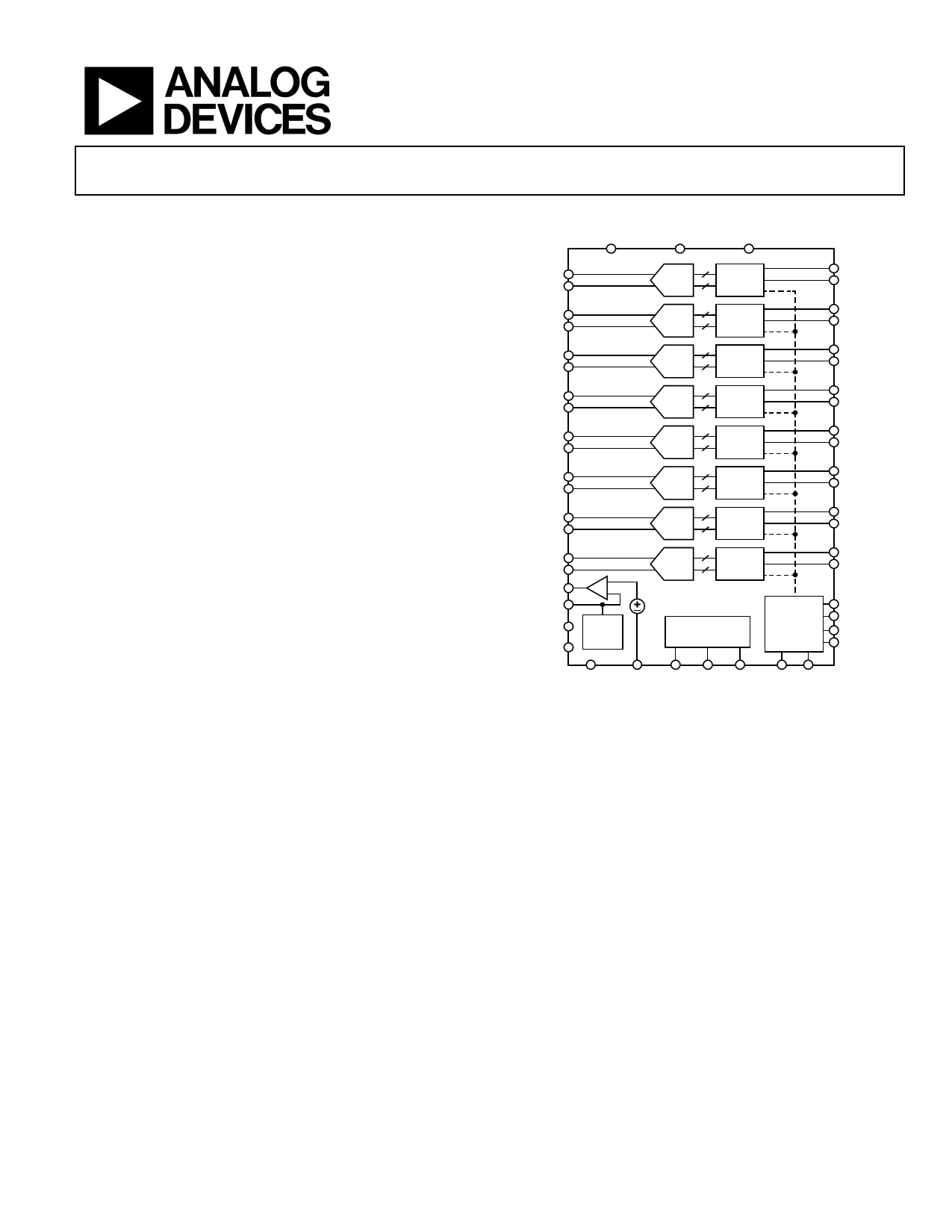
FUNCTIONAL BLOCK DIAGRAM
AVDD
PDWN
DRVDD
AD9637
12
ADC
SERIAL
LVDS
12
ADC
SERIAL
LVDS
12
ADC
SERIAL
LVDS
12
ADC
SERIAL
LVDS
12
ADC
SERIAL
LVDS
12
ADC
SERIAL
LVDS
12
ADC
SERIAL
LVDS
12
ADC
SERIAL
LVDS
D+ A
D– A
D+ B
D– B
D+ C
D– C
D+ D
D– D
D+ E
D– E
D+ F
D– F
D+ G
D– G
D+ H
D– H
REF
SELECT
1.0V
SERIAL PORT
INTERFACE
DATA
RATE
MULTIPLIER
FCO+
FCO–
DCO+
DCO–
RBIAS
AGND
CSB SDIO/ SCLK/
DFS DTP
Figure 1.
CLK+ CLK–
clock and data alignment and programmable digital test pattern
generation. The available digital test patterns include built-in
deterministic and pseudorandom patterns, along with custom user-
defined test patterns entered via the serial port interface (SPI).
The AD9637 is available in a RoHS-compliant, 64-lead LFCSP. It is
specified over the industrial temperature range of −40°C to +85°C.
This product is protected by a U.S. patent.
PRODUCT HIGHLIGHTS
1. Small Footprint. Eight ADCs are contained in a small,
space-saving package.
2. Low Power of 60 mW/Channel at 80 MSPS with Scalable
Power Options.
3. Ease of Use. A data clock output (DCO) is provided that
operates at frequencies of up to 480 MHz and supports
double data rate (DDR) operation.
4. User Flexibility. The SPI control offers a wide range of
flexible features to meet specific system requirements.
5. Pin Compatible with the AD9257 (14-Bit Octal ADC).
One Technology Way, P.O. Box 9106, Norwood, MA 02062-9106, U.S.A.
Tel: 781.329.4700 ©2011–2013 Analog Devices, Inc. All rights reserved.
Technical Support
www.analog.com
1 page 
AD9637
Data Sheet
AC SPECIFICATIONS
AVDD = 1.8 V, DRVDD = 1.8 V, 2 V p-p differential input, 1.0 V internal reference, AIN = −1.0 dBFS, unless otherwise noted. CLK
divider = 8 used for typical characteristics at input frequency ≥ 19.7 MHz.
Table 2.
Parameter1
SIGNAL-TO-NOISE RATIO (SNR)
fIN = 9.7 MHz
fIN = 19.7 MHz
fIN = 30.5 MHz
fIN = 63.5 MHz
fIN = 69.5 MHz
fIN = 123.5 MHz
SIGNAL-TO-NOISE AND DISTORTION RATIO (SINAD)
fIN = 9.7 MHz
fIN = 19.7 MHz
fIN = 30.5 MHz
fIN = 63.5 MHz
fIN = 69.5 MHz
fIN = 123.5 MHz
EFFECTIVE NUMBER OF BITS (ENOB)
fIN = 9.7 MHz
fIN = 19.7 MHz
fIN = 30.5 MHz
fIN = 63.5 MHz
fIN = 69.5 MHz
fIN = 123.5 MHz
SPURIOUS-FREE DYNAMIC RANGE (SFDR)
fIN = 9.7 MHz
fIN = 19.7 MHz
fIN = 30.5 MHz
fIN = 63.5 MHz
fIN = 69.5 MHz
fIN = 123.5 MHz
WORST HARMONIC (SECOND OR THIRD)
fIN = 9.7 MHz
fIN = 19.7 MHz
fIN = 30.5 MHz
fIN = 63.5 MHz
fIN = 69.5 MHz
fIN = 123.5 MHz
WORST OTHER (EXCLUDING SECOND OR THIRD)
fIN = 9.7 MHz
fIN = 19.7 MHz
fIN = 30.5 MHz
fIN = 63.5 MHz
fIN = 69.5 MHz
fIN = 123.5 MHz
TWO-TONE INTERMODULATION DISTORTION (IMD)—
AIN1 AND AIN2 = −7.0 dBFS
fIN1 = 8 MHz, fIN2 = 10 MHz
fIN1 = 30 MHz, fIN2 = 32 MHz
Temp
AD9637-40
Min Typ
Max
25°C 72.0
Full 70.0 72.0
25°C 71.9
25°C
25°C 71.5
25°C
25°C 71.9
Full 69.0 71.9
25°C 71.9
25°C
25°C 71.4
25°C
25°C 11.7
Full 11.2 11.7
25°C 11.7
25°C
25°C 11.6
25°C
25°C
Full 78
25°C
25°C
25°C
25°C
96
96
96
89
25°C −99
Full −96 −78
25°C −98
25°C
25°C −89
25°C
25°C −96
Full −98 −86
25°C −96
25°C
25°C −97
25°C
AD9637-80
Min Typ
Max
71.5
71.0 71.5
71.5
71.4
70.5
71.5
70.0 71.5
71.5
71.3
70.4
11.6
11.3 11.6
11.6
11.6
11.4
93
78 92
92
92
88
−93
−92 −78
−92
−92
−88
−97
−97 −86
−97
−96
−92
Unit
dBFS
dBFS
dBFS
dBFS
dBFS
dBFS
dBFS
dBFS
dBFS
dBFS
dBFS
dBFS
Bits
Bits
Bits
Bits
Bits
Bits
dBc
dBc
dBc
dBc
dBc
dBc
dBc
dBc
dBc
dBc
dBc
dBc
dBc
dBc
dBc
dBc
dBc
dBc
25°C 93
25°C
dBc
85 dBc
Rev. A | Page 4 of 40
5 Page 
AD9637
Pin No.
52, 53
54
55
56
57
58
60, 61
63, 64
Mnemonic
VIN− D, VIN+ D
RBIAS
SENSE
VREF
VCM
SYNC
VIN+ E, VIN− E
VIN− F, VIN+ F
Description
ADC D Analog Input Complement, ADC D Analog Input True.
Sets analog current bias. Connect to 10 kΩ (1% tolerance) resistor to ground.
Reference Mode Selection.
Voltage Reference Input/Output.
Analog Output Voltage at Midsupply. Sets common mode of the analog inputs.
Digital Input. SYNC input to clock divider. 30 kΩ internal pull-down.
ADC E Analog Input True, ADC E Analog Input Complement.
ADC F Analog Input Complement, ADC F Analog Input True.
Data Sheet
Rev. A | Page 10 of 40
11 Page | ||
| Páginas | Total 30 Páginas | |
| PDF Descargar | [ Datasheet AD9637.PDF ] | |
Hoja de datos destacado
| Número de pieza | Descripción | Fabricantes |
| AD9630 | Low Distortion 750 MHz Closed-Loop Buffer Amp | Analog Devices |
| AD9631 | Wide Bandwidth Voltage Feedback Op Amps | Analog Devices |
| AD9632 | Wide Bandwidth Voltage Feedback Op Amps | Analog Devices |
| AD9633 | Serial LVDS 1.8 V ADC | Analog Devices |
| Número de pieza | Descripción | Fabricantes |
| SLA6805M | High Voltage 3 phase Motor Driver IC. |
Sanken |
| SDC1742 | 12- and 14-Bit Hybrid Synchro / Resolver-to-Digital Converters. |
Analog Devices |
|
DataSheet.es es una pagina web que funciona como un repositorio de manuales o hoja de datos de muchos de los productos más populares, |
| DataSheet.es | 2020 | Privacy Policy | Contacto | Buscar |