|
|
|
PDF ADA4961 Data sheet ( Hoja de datos )
| Número de pieza | ADA4961 | |
| Descripción | RF DGA | |
| Fabricantes | Analog Devices | |
| Logotipo | ||
Hay una vista previa y un enlace de descarga de ADA4961 (archivo pdf) en la parte inferior de esta página. Total 25 Páginas | ||
|
No Preview Available !
Data Sheet
Low Distortion, 3.2 GHz, RF DGA
ADA4961
FEATURES
High speed
−3 dB bandwidth: 3.2 GHz
−1 dB bandwidth: 1.8 GHz
Slew rate: 12,000 V/μs
Digitally adjustable gain
Voltage gain: −6 dB to +15 dB
Power gain: −3 dB to +18 dB
5-bit parallel or SPI bus gain control with fast attack
IMD3/HD3 distortion, maximum gain, 5 V, high performance
(HP) mode
IMD3/HD3 at 1 GHz: −90 dBc/−83 dBc
IMD3/HD3 at 1.5 GHz: −85 dBc/−75 dBc
IMD3/HD3 at 2 GHz: −70 dBc/−70 dBc
Low noise
Noise density referred to output (RTO): −154 dBm/Hz
Noise figure: 5.5 dB at AV = 15 dB, 1 GHz
Differential impedances: 100 Ω input, 50 Ω output
Low power mode operation, power-down control
Single 3.3 V or 5 V supply operation
Available in 24-lead, 4 mm × 4 mm LFSCP
APPLICATIONS
ADC driver for 10-bit to 14-bit GSPS converters
RF/IF gain blocks
Line drivers
Instrumentation
Satellite communications
Data acquisition
Military systems
GENERAL DESCRIPTION
The ADA4961 is a high performance, BiCMOS RF digital gain
amplifier (DGA), optimized for driving heavy loads out to
2.0 GHz and beyond. The device typically achieves −90 dBc
IMD3 performance at 500 MHz and −85 dBc at 1.5 GHz. This
RF performance allows GHz converters to achieve their optimum
performance with minimal limitations of the driver amplifier or
constraints on overall power that typically result from GaAs
amplifiers. This device can easily drive 10-bit to16-bit HS
converters.
For many receiver applications, antialias filter (AAF) designs
can be simplified or not required.
The ADA4961 has an internal differential input impedance of
100 Ω and a differential dynamic output impedance of 50 Ω,
eliminating the need for external termination resistors. The
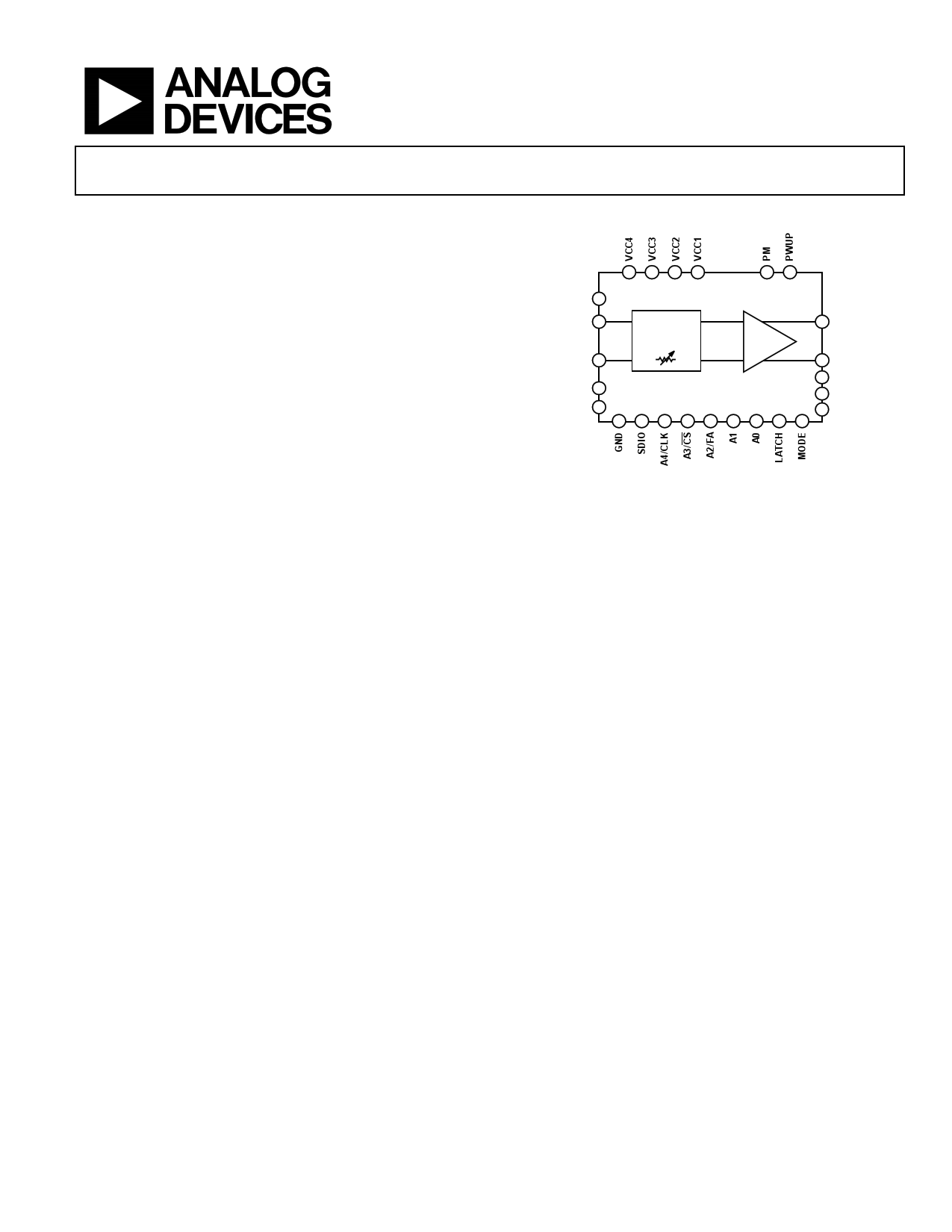
FUNCTIONAL BLOCK DIAGRAM
24 23 22 21
20 19
EXPOSED
PAD
ADA4961
VIN+ 2
0dB TO 21dB
ATTEN
+15dB
17 VOUT+
VIN– 3
16 VOUT–
GND 4
18 DNC
15 DNC
GND 5
14 DNC
1 7 8 9 10 11 12 13 6
NOTES
1. DNC = DO NOT CONNECT. DO NOT CONNECT TO THIS PIN.
Figure 1.
digital adjustability provides for 1 dB resolution, thus optimizing
the signal-to-noise ratio (SNR) for input levels spanning 21 dB.
The ADA4961 is optimized for wideband, low distortion
performance at frequencies up to 2 GHz. These attributes,
together with wide gain adjustment and relatively low power,
make the ADA4961 the amplifier of choice for many high speed
applications, including IF, RF, and broadband applications
where dynamic range at very high frequencies is critical.
The ADA4961 is ideally suited for driving not only analog-to-
digital converters (ADCs), but also mixers, pin diode
attenuators, SAW filters, and multielement discrete devices. It is
available in a 4 mm × 4 mm, 24-lead LFCSP and operates over a
temperature range of −40°C to +85°C.
Rev. A
Document Feedback
Information furnished by Analog Devices is believed to be accurate and reliable. However, no
responsibility is assumed by Analog Devices for its use, nor for any infringements of patents or other
rights of third parties that may result from its use. Specifications subject to change without notice. No
license is granted by implication or otherwise under any patent or patent rights of Analog Devices.
Trademarksandregisteredtrademarksarethepropertyoftheirrespectiveowners.
One Technology Way, P.O. Box 9106, Norwood, MA 02062-9106, U.S.A.
Tel: 781.329.4700
©2014 Analog Devices, Inc. All rights reserved.
Technical Support
www.analog.com
1 page 
ADA4961
Data Sheet
NOISE/HARMONIC PERFORMANCE
VS = 5 V, HP mode, RS = 100 Ω differential,RL = 50 Ω differential, TA = 25°C, f = 500 MHz, VO = 1.2 V p-p(or0.6 V p-pper tone fortwo tone
IMD3), LC filter connected, unlessotherwise noted.
Table 2.
Parameter
AC PERFORMANCE, 100 MHz
Second Harmonic (HD2)
Third Harmonic (HD3)
Third-Order Intermodulation
Distortion (IMD3)
1 dB Compression Point (OP1dB)
Noise Figure (NF)
Noise Density Referred to Output
(RTO)
AC PERFORMANCE, 500 MHz
Second Harmonic (HD2)
Third Harmonic (HD3)
Third-Order Intermodulation
Distortion (IMD3)
1 dB Compression Point (OP1dB)
Noise Figure (NF)
Noise Density Referred to Output
(RTO)
AC PERFORMANCE, 1 GHz
Second Harmonic (HD2)
Third Harmonic (HD3)
Third-Order Intermodulation
Distortion (IMD3)
1 dB Compression Point (OP1dB)
Noise Figure (NF)
Noise Density Referred to Output
(RTO)
AC PERFORMANCE, 1.5 GHz
Second Harmonic (HD2)
Third Harmonic (HD3)
Test Conditions/Comments
Maximum gain
Minimum gain
Maximum gain
Minimum gain
VOUT = 1.2 V p-p composite (2 MHz
spacing)
Maximum gain
Minimum gain
AV = 15 dB
AV = 15 dB
AV = 15 dB
Maximum gain
Minimum gain
Maximum gain
Minimum gain
VOUT = 1.2 V p-p composite (2 MHz
spacing)
Maximum gain
Minimum gain
AV = 15 dB
AV = 15 dB
AV = 15 dB
Maximum gain
Minimum gain
Maximum gain
Minimum gain
VOUT = 1.2 V p-p composite (2 MHz
spacing)
Maximum gain
Minimum gain
AV = 15 dB
AV = 15 dB
AV = 15 dB
Maximum gain
Minimum gain
Maximum gain
Minimum gain
3.3 V Supply, Low
Power Mode
Operation 1
Min Typ Max
5.0 V Supply, High
Performance
Mode Operation
Min Typ Max
Unit
−75 −81 dBc
−76 −80 dBc
−85 −88 dBc
−88 −88 dBc
−100
−95
17.2
6.0
−154
−100
−100
18.8
5.8
−154
dBc
dBc
dBm
dB
dBm/Hz
−77 −80 dBc
−82 −85 dBc
−75 −81 dBc
−75 −82 dBc
−90
−95
17.8
5.8
−154
−90
−90
19.3
5.6
−154
dBc
dBc
dBm
dB
dBm/Hz
−83 −84 dBc
−83 −80 dBc
−78 −83 dBc
−77 −83 dBc
−87
−86
18.1
5.6
−154
−90
−92
21.1
5.5
−154
dBc
dBc
dBm
dB
dBm/Hz
−73 −76 dBc
−75 −77 dBc
−75 −75 dBc
−75 −75 dBc
Rev. A | Page 4 of 24
5 Page 
ADA4961
0
5V, TA = +100°C
3.3V, TA = +100°C
–20
5V, TA = +85°C
3.3V, TA = +85°C
5V, TA = +25°C
3.3V, TA = +25°C
–40 5V, TA = –40°C
3.3V, TA = –40°C
HP
–60
LP
–80
–40
–60
–80
–100
–120
–100
–140
–120
0
–160
200 400 600 800 1000 1200 1400 1600 1800 2000
FREQUENCY (MHz)
Figure 16. IMD3 vs. Frequency at Maximum Gain, Three Temperatures,
5.0 V, 3.3 V, with Low-Pass Filter
–20
5V HP, GAIN = 15, FILTERED
5V HP, GAIN = 15, UNFILTERED
–40 5V HP, GAIN = 7, FILTERED
5V HP, GAIN = 7, UNFILTERED
5V HP, GAIN = 0, FILTERED
–60 5V HP, GAIN = 0, UNFILTERED
–80
–100
–120
–140
0
200 400 600 800 1000 1200 1400 1600 1800 2000
FREQUENCY (MHz)
Figure 17. IMD3 vs. Frequency at 15 dB, 7 dB, and 0 dB Gain Settings, With
and Without Low-Pass Filter, +5.0 V
–60
TA = 25°C
–70
–80
–90
–100
–110
–120
–20
5V HP
3.3V AND 5V LP
–30
5V, GAIN = 15dB
5V, GAIN = 7dB
5V, GAIN = 0dB
3.3V, GAIN = 15dB
3.3V, GAIN = 7dB
3.3V, GAIN = 0dB
–40
–50
–60
–70
–80
–130
–90
–140
0
–100
200 400 600 800 1000 1200 1400 1600 1800 2000
FREQUENCY (MHz)
Figure 18. HD2 vs. Frequency at 15 dB, 7 dB, and 0 dB Gain Settings, +5.0 V,
+3.3 V, with Low-Pass Filter
Data Sheet
–60
TA = 25°C
–70
–80
–90
–100
–110
–120
–20
5V HP
5V, GAIN = 15
5V, GAIN = 7
5V, GAIN = 0
3.3V, GAIN = 15
3.3V, GAIN = 7
3.3V, GAIN = 0
3.3V AND 5V LP
–30
–40
–50
–60
–70
–80
–130
–90
–140
0
–100
200 400 600 800 1000 1200 1400 1600 1800 2000
FREQUENCY (MHz)
Figure 19. HD3 vs. Frequency at 15 dB, 7 dB, and 0 dB Gain Settings, +5.0 V,
+3.3 V, with Low-Pass Filter
–60
GAIN = 15dB
–70
–80
–90
–100
–110
5V HP
3.3V AND 5V LP
–20
–30
–40
5V,
5V,
TTAA
=
=
+85°C
+25°C
5V, TA = –40°C
3.3V, TA = +85°C
3.3V,
3.3V,
TTAA
=
=
+25°C
–40°C
–50
–60
–70
–120
–80
–130
–90
–140
0
–100
200 400 600 800 1000 1200 1400 1600 1800 2000
FREQUENCY (MHz)
Figure 20. HD2 vs. Frequency at Three Temperatures, +5.0 V, +3.3 V, with
Low-Pass Filter
–60
GAIN = 15dB
–70
–80
–90
–100
–110
–120
5V HP
3.3V AND 5V LP
–20
–30
–40
5V,
5V,
TTAA
=
=
+85°C
+25°C
5V, TA = –40°C
3.3V, TA = +85°C
3.3V,
3.3V,
TTAA
=
=
+25°C
–40°C
–50
–60
–70
–80
–130
–90
–140
0
–100
200 400 600 800 1000 1200 1400 1600 1800 2000
FREQUENCY (MHz)
Figure 21. HD3 vs. Frequency at Three Temperatures, 5.0 V, 3.3 V, with
Low-Pass Filter
Rev. A | Page 10 of 24
11 Page | ||
| Páginas | Total 25 Páginas | |
| PDF Descargar | [ Datasheet ADA4961.PDF ] | |
Hoja de datos destacado
| Número de pieza | Descripción | Fabricantes |
| ADA4960-1 | Low Distortion Ultrahigh Speed Differential ADC Driver | Analog Devices |
| ADA4961 | RF DGA | Analog Devices |
| Número de pieza | Descripción | Fabricantes |
| SLA6805M | High Voltage 3 phase Motor Driver IC. |
Sanken |
| SDC1742 | 12- and 14-Bit Hybrid Synchro / Resolver-to-Digital Converters. |
Analog Devices |
|
DataSheet.es es una pagina web que funciona como un repositorio de manuales o hoja de datos de muchos de los productos más populares, |
| DataSheet.es | 2020 | Privacy Policy | Contacto | Buscar |