|
|
|
PDF AD8362 Data sheet ( Hoja de datos )
| Número de pieza | AD8362 | |
| Descripción | 50 Hz to 3.8 GHz 65 dB TruPwr Detector | |
| Fabricantes | Analog Devices | |
| Logotipo | ||
Hay una vista previa y un enlace de descarga de AD8362 (archivo pdf) en la parte inferior de esta página. Total 30 Páginas | ||
|
No Preview Available !
Data Sheet
FEATURES
Complete, fully calibrated measurement/control system
Accurate rms-to-dc conversion from 50 Hz to 3.8 GHz
Input dynamic range of >65 dB: −52 dBm to +8 dBm in 50 Ω
Waveform and modulation independent, such as
GSM/CDMA/TDMA
Linear-in-decibels output, scaled 50 mV/dB
Law conformance error of 0.5 dB
All functions temperature and supply stable
Operates from 4.5 V to 5.5 V at 24 mA
Power-down capability to 1.3 mW
APPLICATIONS
Power amplifier linearization/control loops
Transmitter power controls
Transmitter signal strength indication (TSSI)
Radio frequency (RF) instrumentation
GENERAL DESCRIPTION
The AD8362 is a true rms-responding power detector that has
a 65 dB measurement range. It is intended for use in a variety of
high frequency communication systems and in instrumentation
requiring an accurate response to signal power. It is easy to use,
requiring only a single supply of 5 V and a few capacitors. It
operates from arbitrarily low frequencies to over 3.8 GHz and
accepts inputs from −52 dBm to +8 dBm with crest factors that
are typical of quadrature amplitude modulation (QAM) and
orthogonal frequency division multiplexing (OFDM) modulation
schemes.
The AD8362 has a 1.3 mW power consumption when powered
down by a logic high applied to the PWDN pin. It powers up
within about 20 μs to its nominal operating current of 20 mA at
25°C. The AD8362 is supplied in a 16-lead TSSOP for operation
over the temperature range of −40°C to +85°C.
50 Hz to 3.8 GHz
65 dB TruPwr™ Detector
AD8362
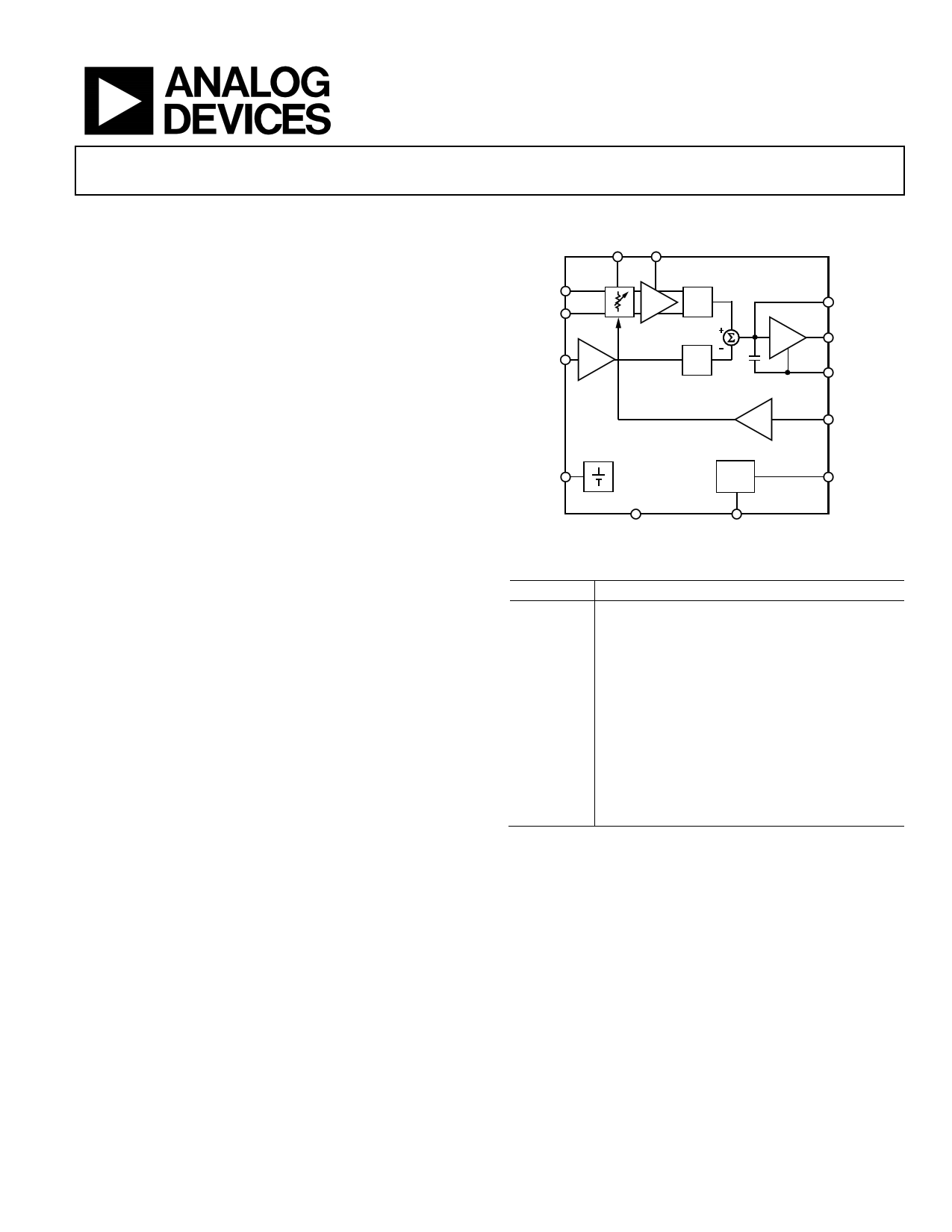
FUNCTIONAL BLOCK DIAGRAM
DECL CHPF
INHI
INLO
VTGT
x2 CLPF
VOUT
x2
ACOM
VREF
AD8362
BIAS
VSET
VPOS
COMM
PWDN
Figure 1.
Table 1. Next Generation Upgrades for the AD8362
Device No. Product Description
ADL5902
Improved temperature stability, single-ended
input drive.
HMC1120
Improved sensitivity and range, includes envelope
tracking and peak-hold function, single-ended
input drive.
ADL5906
Improved temperature stability, single-ended
input drive. Slightly lower input range.
AD8363
Improved temperature stability, single-ended
input drive. Lower input range.
ADL5903
Lower range, significantly lower power consumption,
single-ended input drive.
ADL5501
Lower range, significantly lower power consumption,
linear in V/V output, single-ended input drive.
Rev. F
Document Feedback
Information furnished by Analog Devices is believed to be accurate and reliable. However, no
responsibility is assumed by Analog Devices for its use, nor for any infringements of patents or other
rights of third parties that may result from its use. Specifications subject to change without notice. No
license is granted by implication or otherwise under any patent or patent rights of Analog Devices.
Trademarksandregisteredtrademarksarethepropertyoftheirrespectiveowners.
One Technology Way, P.O. Box 9106, Norwood, MA 02062-9106, U.S.A.
Tel: 781.329.4700 ©2003–2015 Analog Devices, Inc. All rights reserved.
Technical Support
www.analog.com
1 page 
AD8362
Data Sheet
SPECIFICATIONS
VS = 5 V, T = 25°C, ZO = 50 Ω, differential input drive via balun1, VTGT connected to VREF, VOUT tied to VSET, unless otherwise noted.
Table 2.
Parameter
OVERALL FUNCTION
Maximum Input Frequency
Input Power Range (Differential)
Nominal Low End of Range
Nominal High End of Range
Input Voltage Range (Differential)
Nominal Low End of Range
Nominal High End of Range
Input Power Range (S-Sided)
Nominal Low End of Range
Nominal High End of Range
Input Voltage Range (S-Sided)
Nominal Low End of Range
Nominal High End of Range
Input Power Range (S-Sided)
Nominal Low End of Range
Nominal High End of Range
Output Voltage Range
Nominal Low End of Range
Nominal High End of Range
Output Scaling (Log Slope)
Law Conformance Error
RF INPUT INTERFACE
Input Resistance
OUTPUT INTERFACE
Available Output Range
Absolute Voltage Range
Nominal Low End of Range
Nominal High End of Range
Source/Sink Current
Slew Rate Rising
Slew Rate Falling
Rise Time, 10% to 90%
Fall Time, 90% to 10%
Wideband Noise
VSET INTERFACE
Nominal Input Voltage Range
Input Resistance
Scaling (Log Slope)
Scaling (Log Intercept)
VOLTAGE REFERENCE
Output Voltage
Temperature Sensitivity
Output Resistance
Test Conditions/Comments
dB referred to 50 Ω impedance level, f ≤ 2.7 GHz, into 1:4 balun1
RMS voltage at input terminals, f ≤ 2.7 GHz, into input of the device
Single-ended drive, CW input, f ≤ 2.7 GHz, into input resistive network2
RMS voltage at input terminals, f ≤ 2.7 GHz
Single-ended drive, CW input, f ≥ 2.7 GHz, into matched input network3
RL ≥ 200 Ω to ground
In general, VS − 0.1 V
Over central 60 dB range, f ≤ 2.7 GHz
Pin INHI, Pin INLO, ac-coupled, at low frequencies
Single-ended drive, with respect to DECL
Differential drive
Pin VOUT
RL ≥ 200 Ω to ground
Measurement mode, f = 900 MHz, PIN = −52 dBm
Measurement mode, f = 900 MHz, PIN = +8 dBm
VOUT held at VS/2, to 1% change
CL = open
CL = open
0.2 V to 1.8 V, CLPF = Open
1.8 V to 0.2 V, CLPF = Open
CLPF = 1000 pF, fSPOT ≤ 100 kHz
Pin VSET
To ±1 dB error
f = 900 MHz
f = 900 MHz, into 1:4 balun
Pin VREF
25°C
−40°C ≤ TA ≤ +85°C
Min
0.1
0.32
3.44
0.5
46
−64
−77
1.225
Typ
3.8
−52
8
1.12
1.12
−40
0
2.23
2.23
−35
124
100
4.9
50
±0.5
100
200
48
60
5
45
0.4
70
68
50
−60
−73
1.25
0.08
8
Max Unit
GHz
dBm
dBm
mV rms
V rms
dBm
dBm
mV rms
V rms
dBm
dBm
mV
V
mV/dB
dB
Ω
Ω
4.9 V
0.48 V
3.52 V
mA
V/µs
V/µs
ns
µs
nV/√Hz
3.75 V
kΩ
54 mV/dB
−56 dBm
−69 dBV
1.275
V
mV/°C
Ω
Rev. F | Page 4 of 33
5 Page 
AD8362
Data Sheet
TYPICAL PERFORMANCE CHARACTERISTICS
4.5
4.0 100MHz
3.5 2200MHz
3.0
2.5
2.0
1.5 2700MHz
1.0
0.5 900MHz
1900MHz
0–60 –55 –50 –45 –40 –35 –30 –25 –20 –15 –10 –5
0
5 10 15
INPUT AMPLITUDE (dBm)
Figure 8. Output Voltage (VOUT) vs. Input Amplitude (dBm),
Frequencies: 100 MHz, 900 MHz, 1900 MHz, 2200 MHz, and 2700 MHz;
Sine Wave, Differential Drive
3.0
2.5
2.0
1.5
1.0 100MHz
0.5
0
–0.5
–1.0
2200MHz
1900MHz
–1.5 900MHz
–2.0
–2.5 2700MHz
–3.0–60 –55 –50 –45 –40 –35 –30 –25 –20 –15 –10 –5
INPUT AMPLITUDE (dBm)
0
5 10 15
Figure 9. Logarithmic Law Conformance vs. Input Amplitude,
Frequencies: 100 MHz, 900 MHz, 1900 MHz, 2200 MHz, and 2700 MHz;
Sine Wave, Differential Drive
4.0 3.0
3.6 2.4
3.2
2.8 –40°C
1.8
1.2
2.4
+25°C
2.0
1.6 +85°C
1.2 –40°C
0.6
0
–0.6
–1.2
0.8
0.4 +85°C
+25°C
0 –55 –50 –45 –40 –35 –30 –25 –20 –15 –10 –5
INPUT AMPLITUDE (dBm)
0
–1.8
–2.4
5 10 15–3.0
Figure 10. VOUT and Law Conformance vs. Input Amplitude,
Frequency 900 MHz, Sine Wave, Temperatures: −40°C, +25°C, and +85°C
4.0 3.0
3.6 2.4
3.2 1.8
2.8 –40°C
1.2
2.4 0.6
2.0 0
1.6
1.2
+25°C +85°C
–40°C
0.8
+25°C
+85°C
0.4
–0.6
–1.2
–1.8
–2.4
0
–60 –55 –50 –45 –40 –35 –30 –25 –20 –15 –10 –5
INPUT AMPLITUDE (dBm)
0
5 10 15–3.0
Figure 11. VOUT and Law Conformance vs. Input Amplitude,
Frequency 1900 MHz, Sine Wave, Temperatures: −40°C, +25°C, and +85°C
4.0 3.0
3.6 2.4
3.2
2.8 –40°C
1.8
1.2
2.4
2.0
1.6 +25°C
0.6
0
–0.6
1.2
–40°C
0.8
+85°C
0.4 +25°C
+85°C
–1.2
–1.8
–2.4
0
–60 –55 –50 –45 –40 –35 –30 –25 –20 –15 –10 –5 0
INPUT AMPLITUDE (dBm)
5 10 15–3.0
Figure 12. VOUT and Law Conformance vs. Input Amplitude,
Frequency 2200 MHz, Sine Wave, Temperatures: −40°C, +25°C, and +85°C
4.0
3.5
3.0 CW
2.5
IS95 REVERSE LINK
2.0
W-CDMA 8-CHANNEL
1.5 W-CDMA 15-CHANNEL
1.0
0.5
0–60 –55 –50 –45 –40 –35 –30 –25 –20 –15 –10 –5 0
INPUT AMPLITUDE (dBm)
5 10 15
Figure 13. VOUT vs. Input Amplitude with Different Waveforms, CW, IS95
Reverse Link, W-CDMA 8-Channel, W-CDMA 15-Channel, Frequency 900 MHz
Rev. F | Page 10 of 33
11 Page | ||
| Páginas | Total 30 Páginas | |
| PDF Descargar | [ Datasheet AD8362.PDF ] | |
Hoja de datos destacado
| Número de pieza | Descripción | Fabricantes |
| AD8361 | LF to 2.5 GHz TruPwr Detector | Analog Devices |
| AD8362 | 50 Hz to 3.8 GHz 65 dB TruPwr Detector | Analog Devices |
| AD8363 | 50 dB TruPwr Detector | Analog Devices |
| AD8364 | LF to 2.7 GHz Dual 60 dB TruPwr Detector | Analog Devices |
| Número de pieza | Descripción | Fabricantes |
| SLA6805M | High Voltage 3 phase Motor Driver IC. |
Sanken |
| SDC1742 | 12- and 14-Bit Hybrid Synchro / Resolver-to-Digital Converters. |
Analog Devices |
|
DataSheet.es es una pagina web que funciona como un repositorio de manuales o hoja de datos de muchos de los productos más populares, |
| DataSheet.es | 2020 | Privacy Policy | Contacto | Buscar |