|
|
|
PDF AD8347 Data sheet ( Hoja de datos )
| Número de pieza | AD8347 | |
| Descripción | 0.8 GHz to 2.7 GHz Direct Conversion Quadrature Demodulator | |
| Fabricantes | Analog Devices | |
| Logotipo | ||
Hay una vista previa y un enlace de descarga de AD8347 (archivo pdf) en la parte inferior de esta página. Total 29 Páginas | ||
|
No Preview Available !
0.8 GHz to 2.7 GHz Direct Conversion
Quadrature Demodulator
AD8347
FEATURES
Integrated RF and baseband AGC amplifiers
Quadrature phase accuracy 1° typ
I/Q amplitude balance 0.3 dB typ
Third-order intercept (IIP3) +11.5 dBm @ min gain
Noise figure 11 dB @ max gain
AGC range 69.5 dB
Baseband level control circuit
Low LO drive −8 dBm
ADC-compatible I/Q outputs
Single supply 2.7 V to 5.5 V
Power-down mode
28-lead TSSOP package
APPLICATIONS
Cellular base stations
Radio links
Wireless local loop
IF broadband demodulators
RF instrumentation
Satellite modems
GENERAL DESCRIPTION
The AD83471 is a broadband direct quadrature demodulator
with RF and baseband automatic gain control (AGC) amplifiers.
It is suitable for use in many communications receivers, performing
quadrature demodulation directly to baseband frequencies. The
input frequency range is 800 MHz to 2.7 GHz. The outputs can
be connected directly to popular A-to-D converters such as the
AD9201 and AD9283.
The RF input signal goes through two stages of variable gain
amplifiers prior to two Gilbert-cell mixers. The LO quadrature
phase splitter employs polyphase filters to achieve high
quadrature accuracy and amplitude balance over the entire
operating frequency range. Separate I and Q channel variable
gain amplifiers follow the baseband outputs of the mixers. The
RF and baseband amplifiers together provide 69.5 dB of gain
control. A precision control circuit sets the linear-in-dB RF gain
response to the gain control voltage.
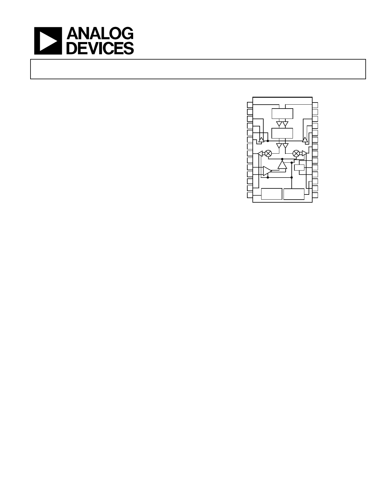
FUNCTIONAL BLOCK DIAGRAM
LOIN 1
VPS1 2
IOPN 3
IOPP 4
VCMO 5
IAIN 6
COM3 7
IMXO 8
COM2 9
RFIN 10
RFIP 11
VPS2 12
IOFS 13
VREF 14
AD8347
PHASE
SPLITTER
PHASE
SPLITTER
DET
BIAS
GAIN
CONTROL
Figure 1.
28 LOIP
27 COM1
26 QOPN
25 QOPP
24 QAIN
23 COM3
22 QMXO
21 VPS3
20 VDT1
19 VAGC
18 VDT2
17 VGIN
16 QOFS
15 ENBL
Baseband level detectors are included for use in an AGC loop to
maintain the output level. The demodulator dc offsets are
minimized by an internal loop, whose time constant is
controlled by external capacitor values. The offset control can
also be overridden by forcing an external voltage at the offset
nulling pins.
The baseband variable gain amplifier outputs are brought off-
chip for filtering before final amplification. By inserting a
channel selection filter before each output amplifier, high level
out-of-channel interferers are eliminated. Additional internal
circuitry also allows the user to set the dc common-mode level
at the baseband outputs.
1 U.S. patents issued and pending.
Rev. A
Information furnished by Analog Devices is believed to be accurate and reliable. However, no
responsibility is assumed by Analog Devices for its use, nor for any infringements of patents or other
rights of third parties that may result from its use. Specifications subject to change without notice. No
license is granted by implication or otherwise under any patent or patent rights of Analog Devices.
Trademarksandregisteredtrademarksarethepropertyoftheirrespectiveowners.
One Technology Way, P.O. Box 9106, Norwood, MA 02062-9106, U.S.A.
Tel: 781.329.4700
www.analog.com
Fax: 781.461.3113
© 2005 Analog Devices, Inc. All rights reserved.
1 page 
AD8347
Parameter
CONTROL INPUT/OUTPUTS
VCMO Input
Gain Control Input Bias Current
Offset Input Overriding Current
VREF Output
RESPONSE FROM RF INPUT TO FINAL
BB AMP
Gain @ VVGIN = 0.2 V
Gain @ VVGIN = 1.2 V
Gain Slope
Gain Intercept
LO/RF INPUT
LOIP Input Return Loss
RFIP Input Return Loss
ENABLE
Power-Up Control
Power-Up Control
Power-Up Time
Power-Down Time
POWER SUPPLIES
Voltage
Current (Enabled)
Current (Standby)
Current (Standby)
Conditions
Min Typ
@ VS = 2.7 V
@ VS = 5 V
VGIN
IOFS, QOFS
RLOAD = 10 kΩ
IMXO and QMXO connected directly to IAIN and QAIN,
respectively
Linear extrapolation back to theoretical value at VGIN = 0
(See Figure 30 through Figure 33 for more detail)
Measuring LOIP LOIN, ac-coupled to ground with 100 pF.
Measuring through evaluation board balun with termination
RFIP input pin
0.5
0.95
65.5
−3
−96.5
88
1
1
<1
10
1.00
69.5
+0.5
−89
94
−4
−9.5
−10
Low = standby
High = enabled
Time for final BB amps to be within 90% of final amplitude
@ VS = 5 V
@ VS = 2.7 V
Time for supply current to be <4 mA
@ VS = 5 V
@ VS = 2.7 V
VPS1, VPS2, VPS3
@5V
@5V
@ 3.3 V
0
+VS − 1
20
10
30
1.5
2.7
48 64
400
80
Max Unit
V
2.5 V
μA
μA
1.05 V
72.5
+4
−82.5
101
dB
dB
dB/V
dB
dB
dB
dB
0.5 V
+VS V
μs
μs
μs
ms
5.5 V
80 mA
μA
μA
Rev. A | Page 4 of 28
5 Page 
AD8347
–10
–12
–14
VS = 5V, TA = +85°C
–16
–18 VS = 2.7V, TA = +85°C
–20
–22 VS = 5V, TA = +25°C
–24 VS = 5V, TA = –40°C
–26 VS = 2.7V, TA = +25°C
–28
–30
–32 VS = 2.7V,
TA = –40°C
–34
0 5 10 15 20 25 30 35 40 45 50 55 60 65 70 75 80 85 90 95 100
BASEBAND FREQUENCY (MHz)
Figure 16. IIP3 vs. FBB, VVGIN = 0.2 V, FLO = 1900 MHz
50
45
40
35
30
25
20
800 1000 1200 1400 1600 1800 2000 2200 2400 2600
RF FREQUENCY (MHz)
Figure 17. IIP2 vs. FLO, VVGIN = 1.2 V, Baseband Tone1 = 5 MHz, −10 dBm,
Baseband Tone2 = 6 MHz, −10 dBm, Temperature = 25°C, VS = 5 V
13.0
12.5
12.0
11.5
11.0
10.5
VS = 5V
VS = 2.7V
10.0
800 1000 1200 1400 1600 1800 2000 2200 2400 2600
LO FREQUENCY (MHz)
Figure 18. Noise Figure vs. LO Frequency (FLO), Temperature = 25°C,
VVGIN = 0.2 V, FBB = 1 MHz
70 15
10
60
5
50
0
40 –5
30 VS = 5V
–10
20 VS = 2.7V
–15
–20
10
VS = 2.7V
0 VS = 5V
–25
–30
0.2 0.3 0.4 0.5 0.6 0.7 0.8 0.9 1.0
VVGIN (V)
Figure 19. Noise Figure and IIP3 vs. VVGIN, Temperature = 25°C,
FLO = 1900 MHz, FBB = 1 MHz
2.5
2.0
1.5
1.0
0.5
LO FREQUENCY = 2700MHz
0
–0.5
–1.0
LO FREQUENCY = 800MHz
–1.5
LO FREQUENCY = 1900MHz
–2.0
–2.5
–20 –18 –16 –14 –12 –10 –8 –6 –4 –2
LO INPUT LEVEL (dBm)
0
Figure 20. Quadrature Error vs. LO Power Level, Temperature = 25°C,
VVGIN = 0.2 V, VS = 5 V
14.0
13.5
13.0
12.5
12.0
2700MHz
11.5
11.0
1900MHz
10.5
10.0 800MHz
9.5
9.0
–20 –18 –16 –14 –12 –10 –8 –6 –4 –2
LO INPUT LEVEL (dBm)
0
Figure 21. Noise Figure vs. LO Input Level, Temperature = 25°C,
VVGIN = 0.2 V, VS = 5 V
Rev. A | Page 10 of 28
11 Page | ||
| Páginas | Total 29 Páginas | |
| PDF Descargar | [ Datasheet AD8347.PDF ] | |
Hoja de datos destacado
| Número de pieza | Descripción | Fabricantes |
| AD834 | 500 MHz Four-Quadrant Multiplier | Analog Devices |
| AD8340 | RF Vector Modulator | Analog Devices |
| AD8341 | 1.5GHz to 2.4GHz RF Vector Modulator | Analog Devices |
| AD8342 | Active Receive Mixer Low Frequency to 3.8 GHz | Analog Devices |
| Número de pieza | Descripción | Fabricantes |
| SLA6805M | High Voltage 3 phase Motor Driver IC. |
Sanken |
| SDC1742 | 12- and 14-Bit Hybrid Synchro / Resolver-to-Digital Converters. |
Analog Devices |
|
DataSheet.es es una pagina web que funciona como un repositorio de manuales o hoja de datos de muchos de los productos más populares, |
| DataSheet.es | 2020 | Privacy Policy | Contacto | Buscar |