|
|
|
PDF AD9520-2 Data sheet ( Hoja de datos )
| Número de pieza | AD9520-2 | |
| Descripción | 12 LVPECL/24 CMOS Output Clock Generator | |
| Fabricantes | Analog Devices | |
| Logotipo | ||
Hay una vista previa y un enlace de descarga de AD9520-2 (archivo pdf) en la parte inferior de esta página. Total 30 Páginas | ||
|
No Preview Available !
Data Sheet
12 LVPECL/24 CMOS Output Clock
Generator with Integrated 2.2 GHz VCO
AD9520-2
FEATURES
Low phase noise, phase-locked loop (PLL)
On-chip VCO tunes from 2.02 GHz to 2.335 GHz
Optional external 3.3 V/5 V VCO/VCXO to 2.4 GHz
1 differential or 2 single-ended reference inputs
Accepts CMOS, LVDS, or LVPECL references to 250 MHz
Accepts 16.62 MHz to 33.3 MHz crystal for reference input
Optional reference clock doubler
Reference monitoring capability
Automatic/manual reference holdover and reference
switchover modes, with revertive switching
Glitch-free switchover between references
Automatic recovery from holdover
Digital or analog lock detect, selectable
Optional zero delay operation
Twelve 1.6 GHz LVPECL outputs divided into 4 groups
Each group of 3 outputs shares a 1-to-32 divider with
phase delay
Additive output jitter as low as 225 fs rms
Channel-to-channel skew grouped outputs < 16 ps
Each LVPECL output can be configured as 2 CMOS outputs
(for fOUT ≤ 250 MHz)
Automatic synchronization of all outputs on power-up
Manual output synchronization available
SPI- and I²C-compatible serial control port
64-lead LFCSP
Nonvolatile EEPROM stores configuration settings
APPLICATIONS
Low jitter, low phase noise clock distribution
Clock generation and translation for SONET, 10Ge, 10GFC,
Synchronous Ethernet, OTU2/3/4
Forward error correction (G.710)
Clocking high speed ADCs, DACs, DDSs, DDCs, DUCs, MxFEs
High performance wireless transceivers
ATE and high performance instrumentation
Broadband infrastructures
GENERAL DESCRIPTION
The AD9520-21 provides a multioutput clock distribution
function with subpicosecond jitter performance, along with an
on-chip PLL and VCO. The on-chip VCO tunes from 2.02 GHz
to 2.335 GHz. An external 3.3 V/5 V VCO/VCXO of up to 2.4 GHz
can also be used.
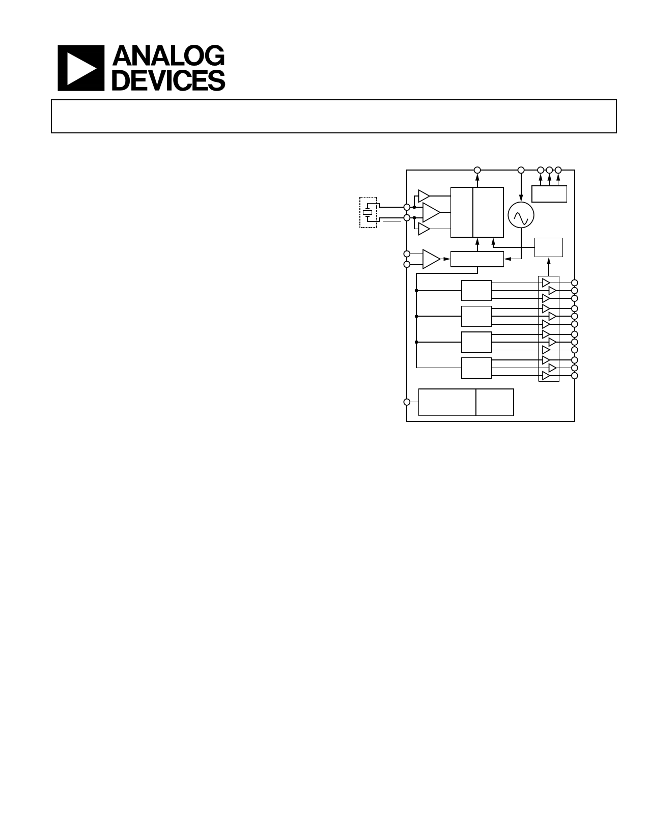
FUNCTIONAL BLOCK DIAGRAM
CP LF
OPTIONAL
REFIN
REFIN
CLK
REF1
REF2
STATUS
MONITOR
VCO
DIVIDER
AND MUXES
DIV/Φ
DIV/Φ
DIV/Φ
DIV/Φ
ZERO
DELAY
LVPECL/
CMOS
OUT0
OUT1
OUT2
OUT3
OUT4
OUT5
OUT6
OUT7
OUT8
OUT9
OUT10
OUT11
SPI/I2C CONTROL
PORT AND
EEPROM
DIGITAL LOGIC
AD9520
Figure 1.
The AD9520-2 serial interface supports both SPI and I²C ports.
An in-package EEPROM, which can be programmed through the
serial interface, can store user-defined register settings for
power-up and chip reset.
The AD9520-2 features 12 LVPECL outputs in four groups. Any
of the 1.6 GHz LVPECL outputs can be reconfigured as two
250 MHz CMOS outputs. If an application requires LVDS
drivers instead of LVPECL drivers, refer to the AD9522-2.
Each group of three outputs has a divider that allows both the
divide ratio (from 1 to 32) and the phase offset or coarse time
delay to be set.
The AD9520-2 is available in a 64-lead LFCSP and can be operated
from a single 3.3 V supply. The external VCO can have an
operating voltage of up to 5.5 V. A separate output driver power
supply can be from 2.375 V to 3.465 V.
The AD9520-2 is specified for operation over the standard
industrial range of −40°C to +85°C.
1AD9520 is used throughout this data sheet to refer to all the members of the AD9520 family. However, when AD9520-2 is used, it refers to that specific member of the
AD9520 family.
Rev. B
Document Feedback
Information furnished by Analog Devices is believed to be accurate and reliable. However, no
responsibilityisassumedbyAnalogDevices for itsuse,nor foranyinfringementsofpatentsor other
rights of third parties that may result from its use. Specifications subject to change without notice. No
license is granted by implication or otherwise under any patent or patent rights of Analog Devices.
Trademarksandregisteredtrademarksarethepropertyoftheirrespectiveowners.
One Technology Way, P.O. Box 9106, Norwood, MA 02062-9106, U.S.A.
Tel: 781.329.4700 ©2008–2016 Analog Devices, Inc. All rights reserved.
Technical Support
www.analog.com
1 page 
AD9520-2
Data Sheet
SPECIFICATIONS
Typical is given for VS= VS_DRV = 3.3 V ± 5%; VS ≤ VCP ≤ 5.25 V; TA = 25°C; RSET = 4.12 kΩ; CPRSET = 5.1 kΩ, unless otherwise noted. Minimum
and maximum values are given over full VS and TA (−40°C to +85°C) variation.
POWER SUPPLY REQUIREMENTS
Table 1.
Parameter
POWER PINS
VS
VS_DRV
VCP
CURRENT SET RESISTORS
RSET Pin Resistor
CPRSET Pin Resistor
BYPASS PIN CAPACITOR
PLL CHARACTERISTICS
Min Typ
3.135
2.375
VS
3.3
4.12
5.1
220
Max
3.465
VS
5.25
Unit
V
V
V
kΩ
kΩ
nF
Test Conditions/Comments
3.3 V ± 5%
Nominally 2.5 V to 3.3 V ± 5%
Nominally 3.3 V to 5.0 V ± 5%
Sets internal biasing currents; connect to ground
Sets internal CP current range, nominally 4.8 mA
(CP_lsb = 600 µA); actual current can be calculated
by CP_lsb = 3.06/CPRSET; connect to ground
Bypass for internal LDO regulator; necessary for LDO
stability; connect to ground
Table 2.
Parameter
VCO (ON CHIP)
Frequency Range
VCO Gain (KVCO)
Tuning Voltage (VT)
Frequency Pushing (Open-Loop)
Phase Noise at 1 kHz Offset
Phase Noise at 100 kHz Offset
Phase Noise at 1 MHz Offset
REFERENCE INPUTS
Differential Mode (REFIN, REFIN)
Input Frequency
Input Sensitivity
Self-Bias Voltage, REFIN
Self-Bias Voltage, REFIN
Input Resistance, REFIN
Input Resistance, REFIN
Dual Single-Ended Mode (REF1, REF2)
Input Frequency (AC-Coupled with
DC Offset Off)
Input Frequency (AC-Coupled with
DC Offset On)
Input Frequency (DC-Coupled)
Input Sensitivity (AC-Coupled with
DC Offset Off)
Input Sensitivity (AC-Coupled with
DC Offset On)
Input Logic High, DC Offset Off
Input Logic Low, DC Offset Off
Input Current
Input Capacitance
Min Typ
Max Unit Test Conditions/Comments
2020
0.5
38
1
−52
−108
−128
2335
VCP − 0.5
MHz
MHz/V
V
MHz/V
dBc/Hz
dBc/Hz
dBc/Hz
See Figure 8
VT ≤ VS when using internal VCO
f = 2175 MHz
f = 2175 MHz
f = 2175 MHz
0
1.35
1.30
4.0
4.4
10
0
0.55
1.5
2.0
−100
Differential mode (can accommodate single-ended
input by ac grounding undriven input)
250 MHz Frequencies below about 1 MHz should be dc-coupled;
be careful to match VCM (self-bias voltage)
280 mV p-p PLL figure of merit (FOM) increases with increasing slew
rate (see Figure 12); the input sensitivity is sufficient for
ac-coupled LVDS and LVPECL signals
1.60 1.75 V
Self-bias voltage of REFIN1
1.50 1.60 V
Self-bias voltage of REFIN1
4.8 5.9 kΩ Self-biased1
5.3 6.4 kΩ Self-biased1
Two single-ended CMOS-compatible inputs
250 MHz Slew rate must be > 50 V/µs
250 MHz Slew rate must be > 50 V/µs, and input amplitude
sensitivity specification must be met; see the input
sensitivity parameter
250 MHz Slew rate > 50 V/µs; CMOS levels
3.28
V p-p
VIH should not exceed VS
2.78
V p-p
VIH should not exceed VS
V
0.8 V
+100
µA
2 pF
Rev. B | Page 4 of 80
Each pin, REFIN (REF1)/REFIN (REF2)
5 Page 
AD9520-2
Data Sheet
CLOCK OUTPUT ADDITIVE PHASE NOISE (DISTRIBUTION ONLY; VCO DIVIDER NOT USED)
Table 6.
Parameter
Min Typ Max Unit
Test Conditions/Comments
CLK-TO-LVPECL ADDITIVE PHASE NOISE
Distribution section only; does not include PLL and VCO
CLK = 1 GHz, Output = 1 GHz
Input slew rate > 1 V/ns
Divider = 1
10 Hz Offset
−107
dBc/Hz
100 Hz Offset
−117
dBc/Hz
1 kHz Offset
−127
dBc/Hz
10 kHz Offset
−135
dBc/Hz
100 kHz Offset
−142
dBc/Hz
1 MHz Offset
−145
dBc/Hz
10 MHz Offset
−147
dBc/Hz
100 MHz Offset
−150
dBc/Hz
CLK = 1 GHz, Output = 200 MHz
Input slew rate > 1 V/ns
Divider = 5
10 Hz Offset
−122
dBc/Hz
100 Hz Offset
−132
dBc/Hz
1 kHz Offset
−143
dBc/Hz
10 kHz Offset
−150
dBc/Hz
100 kHz Offset
−156
dBc/Hz
1 MHz Offset
−157
dBc/Hz
>10 MHz Offset
−157
dBc/Hz
CLK-TO-CMOS ADDITIVE PHASE NOISE
Distribution section only; does not include PLL and VCO
CLK = 1 GHz, Output = 250 MHz
Input slew rate > 1 V/ns
Divider = 4
10 Hz Offset
−107
dBc/Hz
100 Hz Offset
−119
dBc/Hz
1 kHz Offset
−125
dBc/Hz
10 kHz Offset
−134
dBc/Hz
100 kHz Offset
−144
dBc/Hz
1 MHz Offset
−148
dBc/Hz
>10 MHz Offset
−154
dBc/Hz
CLK = 1 GHz, Output = 50 MHz
Input slew rate > 1 V/ns
Divider = 20
10 Hz Offset
−126
dBc/Hz
100 Hz Offset
−133
dBc/Hz
1 kHz Offset
−140
dBc/Hz
10 kHz Offset
−148
dBc/Hz
100 kHz Offset
−157
dBc/Hz
1 MHz Offset
−160
dBc/Hz
>10 MHz Offset
−163
dBc/Hz
Rev. B | Page 10 of 80
11 Page | ||
| Páginas | Total 30 Páginas | |
| PDF Descargar | [ Datasheet AD9520-2.PDF ] | |
Hoja de datos destacado
| Número de pieza | Descripción | Fabricantes |
| AD9520-0 | 12 LVPECL/24 CMOS Output Clock Generator | Analog Devices |
| AD9520-1 | 12 LVPECL/24 CMOS Output Clock Generator | Analog Devices |
| AD9520-2 | 12 LVPECL/24 CMOS Output Clock Generator | Analog Devices |
| AD9520-3 | 12 LVPECL/24 CMOS Output Clock Generator | Analog Devices |
| Número de pieza | Descripción | Fabricantes |
| SLA6805M | High Voltage 3 phase Motor Driver IC. |
Sanken |
| SDC1742 | 12- and 14-Bit Hybrid Synchro / Resolver-to-Digital Converters. |
Analog Devices |
|
DataSheet.es es una pagina web que funciona como un repositorio de manuales o hoja de datos de muchos de los productos más populares, |
| DataSheet.es | 2020 | Privacy Policy | Contacto | Buscar |