|
|
|
PDF AD9744 Data sheet ( Hoja de datos )
| Número de pieza | AD9744 | |
| Descripción | D/A Converter | |
| Fabricantes | Analog Devices | |
| Logotipo | ||
Hay una vista previa y un enlace de descarga de AD9744 (archivo pdf) en la parte inferior de esta página. Total 30 Páginas | ||
|
No Preview Available !
Data Sheet
FEATURES
High performance member of pin-compatible
TxDAC product family
Excellent spurious-free dynamic range performance
SFDR to Nyquist
83 dBc at 5 MHz output
80 dBc at 10 MHz output
73 dBc at 20 MHz output
SNR at 5 MHz output, 125 MSPS: 77 dB
Twos complement or straight binary data format
Differential current outputs: 2 mA to 20 mA
Power dissipation: 135 mW at 3.3 V
Power-down mode: 15 mW at 3.3 V
On-chip 1.2 V reference
CMOS-compatible digital interface
28-lead SOIC, 28-lead TSSOP, and 32-lead LFCSP packages
Edge-triggered latches
GENERAL DESCRIPTION
The AD97441 is a 14-bit resolution, wideband, third generation
member of the TxDAC series of high performance, low power
CMOS digital-to-analog converters (DACs). The TxDAC family,
consisting of pin-compatible 8-, 10-, 12-, and 14-bit DACs, is
specifically optimized for the transmit signal path of communi-
cation systems. All of the devices share the same interface options,
small outline package, and pinout, providing an upward or
downward component selection path based on performance,
resolution, and cost. The AD9744 offers exceptional ac and dc
performance while supporting update rates up to 210 MSPS.
The AD9744’s low power dissipation makes it well suited for
portable and low power applications. Its power dissipation can
be further reduced to a mere 60 mW with a slight degradation
in performance by lowering the full-scale current output. Also,
a power-down mode reduces the standby power dissipation to
approximately 15 mW. A segmented current source architecture
is combined with a proprietary switching technique to reduce
spurious components and enhance dynamic performance.
Rev. C
Document Feedback
Information furnished by Analog Devices is believed to be accurate and reliable. However, no
responsibility is assumed by Analog Devices for its use, nor for any infringements of patents or other
rights of third parties that may result from its use. Specifications subject to change without notice. No
license is granted by implication or otherwise under any patent or patent rights of Analog Devices.
Trademarksandregisteredtrademarksarethepropertyoftheirrespectiveowners.
14-Bit, 210 MSPS TxDAC®
D/A Converter
AD9744
APPLICATIONS
Wideband communication transmit channel
Direct IFs
Base stations
Wireless local loops
Digital radio links
Direct digital synthesis (DDS)
Instrumentation
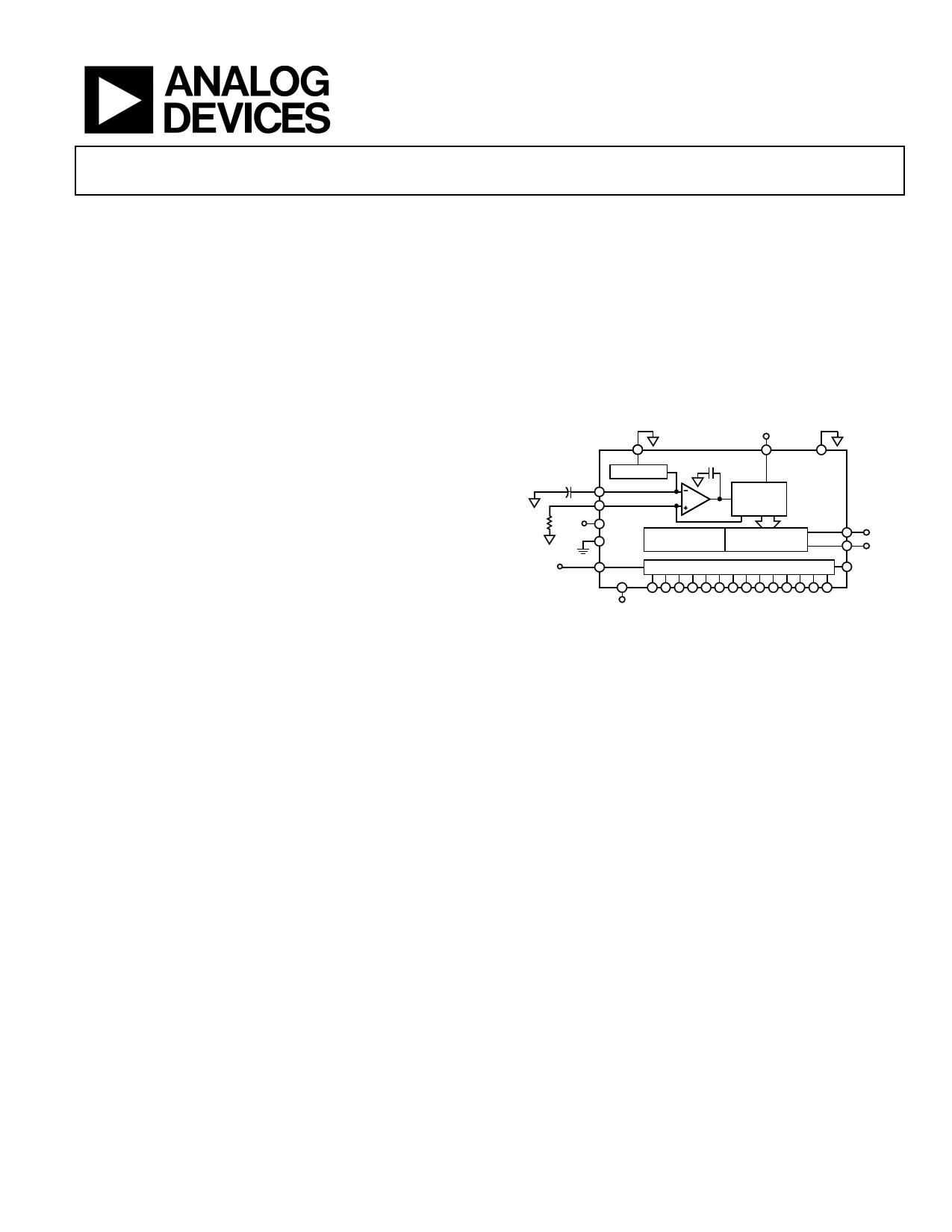
FUNCTIONAL BLOCK DIAGRAM
3.3V
0.1µF
RSET 3.3V
CLOCK
REFLO
1.2V REF
REFIO
FS ADJ
150pF
AVDD ACOM
CURRENT AD9744
SOURCE
ARRAY
DVDD
DCOM
SEGMENTED
SWITCHES
LSB
SWITCHES
IOUTA
IOUTB
CLOCK
LATCHES
MODE
SLEEP
DIGITAL DATA INPUTS (DB13–DB0)
Figure 1.
Edge-triggered input latches and a 1.2 V temperature compensated
band gap reference have been integrated to provide a complete
monolithic DAC solution. The digital inputs support 3 V
CMOS logic families.
PRODUCT HIGHLIGHTS
1. The AD9744 is the 14-bit member of the pin compatible TxDAC
family, which offers excellent INL and DNL performance.
2. Data input supports twos complement or straight binary data
coding.
3. High speed, single-ended CMOS clock input supports
210 MSPS conversion rate.
4. Low power: Complete CMOS DAC function operates on
135 mW from a 2.7 V to 3.6 V single supply. The DAC full-
scale current can be reduced for lower power operation, and a
sleep mode is provided for low power idle periods.
5. On-chip voltage reference: The AD9744 includes a 1.2 V
temperature compensated band gap voltage reference.
6. Industry-standard 28-lead SOIC, 28-lead TSSOP, and 32-lead
LFCSP packages.
1Protected by U.S. Patent Numbers 5568145, 5689257, and 5703519.
One Technology Way, P.O. Box 9106, Norwood, MA 02062-9106, U.S.A.
Tel: 781.329.4700 ©2003–2013 Analog Devices, Inc. All rights reserved.
Technical Support
www.analog.com
1 page 
AD9744
Data Sheet
DYNAMIC SPECIFICATIONS
TMIN to TMAX, AVDD = 3.3 V, DVDD = 3.3 V, CLKVDD = 3.3 V, IOUTFS = 20 mA, differential transformer coupled output, 50 Ω doubly
terminated, unless otherwise noted.
Table 2.
Parameter
DYNAMIC PERFORMANCE
Maximum Output Update Rate (fCLOCK)
Output Settling Time (tST) (to 0.1%)1
Output Propagation Delay (tPD)
Glitch Impulse
Output Rise Time (10% to 90%)1
Output Fall Time (10% to 90%)1
Output Noise (IOUTFS = 20 mA)2
Output Noise (IOUTFS = 2 mA)2
Noise Spectral Density3
AC LINEARITY
Spurious-Free Dynamic Range to Nyquist
fCLOCK = 25 MSPS; fOUT = 1.00 MHz
0 dBFS Output
−6 dBFS Output
−12 dBFS Output
−18 dBFS Output
fCLOCK = 65 MSPS; fOUT = 1.00 MHz
fCLOCK = 65 MSPS; fOUT = 2.51 MHz
fCLOCK = 65 MSPS; fOUT = 10 MHz
fCLOCK = 65 MSPS; fOUT = 15 MHz
fCLOCK = 65 MSPS; fOUT = 25 MHz
fCLOCK = 165 MSPS; fOUT = 21 MHz
fCLOCK = 165 MSPS; fOUT = 41 MHz
fCLOCK = 210 MSPS; fOUT = 41 MHz
fCLOCK = 210 MSPS; fOUT = 69 MHz
Spurious-Free Dynamic Range Within a Window
fCLOCK = 25 MSPS; fOUT = 1.00 MHz; 2 MHz Span
fCLOCK = 50 MSPS; fOUT = 5.02 MHz; 2 MHz Span
fCLOCK = 65 MSPS; fOUT = 5.03 MHz; 2.5 MHz Span
fCLOCK = 125 MSPS; fOUT = 5.04 MHz; 4 MHz Span
Total Harmonic Distortion
fCLOCK = 25 MSPS; fOUT = 1.00 MHz
fCLOCK = 50 MSPS; fOUT = 2.00 MHz
fCLOCK = 65 MSPS; fOUT = 2.00 MHz
fCLOCK = 125 MSPS; fOUT = 2.00 MHz
Signal-to-Noise Ratio
fCLOCK = 65 MSPS; fOUT = 5 MHz; IOUTFS = 20 mA
fCLOCK = 65 MSPS; fOUT = 5 MHz; IOUTFS = 5 mA
fCLOCK = 125 MSPS; fOUT = 5 MHz; IOUTFS = 20 mA
fCLOCK = 125 MSPS; fOUT = 5 MHz; IOUTFS = 5 mA
fCLOCK = 165 MSPS; fOUT = 5 MHz; IOUTFS = 20 mA
fCLOCK = 165 MSPS; fOUT = 5 MHz; IOUTFS = 5 mA
fCLOCK = 210 MSPS; fOUT = 5 MHz; IOUTFS = 20 mA
fCLOCK = 210 MSPS; fOUT = 5 MHz; IOUTFS = 5 mA
Min Typ
Max Unit
210
11
1
5
2.5
2.5
50
30
−155
MSPS
ns
ns
pV-s
ns
ns
pA/√Hz
pA/√Hz
dBm/Hz
77 90
87
82
82
85
84
80
75
74
73
60
68
64
dBc
dBc
dBc
dBc
dBc
dBc
dBc
dBc
dBc
dBc
dBc
dBc
dBc
84 90
90
87
87
dBc
dBc
dBc
dBc
−86 −77 dBc
−77 dBc
−77 dBc
−77 dBc
82 dB
88 dB
77 dB
78 dB
70 dB
70 dB
74 dB
67 dB
Rev. C | Page 4 of 32
5 Page 
AD9744
95
90 4MHz
85
80
75
19MHz
70
65
34MHz
60
55
49MHz
50
45
–40
–20
0
20 40 60 80
TEMPERATURE (°C)
Figure 17. SFDR vs. Temperature at 165 MSPS, 0 dBFS
0
–10
–20
–30
–40
–50
–60
–70
–80
–90
–100
1
fCLOCK = 78MSPS
fOUT = 15.0MHz
SFDR = 79dBc
AMPLITUDE = 0dBFS
6 11 16 21 26 31 36
FREQUENCY (MHz)
Figure 18. Single-Tone SFDR
0
–10
–20
–30
–40
–50
–60
–70
–80
–90
–100
1
fCLOCK = 78MSPS
fOUT1 = 15.0MHz
fOUT2 = 15.4MHz
SFDR = 77dBc
AMPLITUDE = 0dBFS
6 11 16 21 26 31 36
FREQUENCY (MHz)
Figure 19. Dual-Tone SFDR
Data Sheet
0
–10
–20
–30
–40
–50
–60
–70
–80
–90
–100
1
fCLOCK = 78MSPS
fOUT1 = 15.0MHz
fOUT2 = 15.4MHz
fOUT3 = 15.8MHz
fOUT4 = 16.2MHz
SFDR = 75dBc
AMPLITUDE = 0dBFS
6 11 16 21 26 31 36
FREQUENCY (MHz)
Figure 20. Four-Tone SFDR
–20
–39.01dBm
–30
29.38000000MHz
CHPWR –19.26dBm
ACP UP –64.98dB
–40 ACP LOW +0.55dB
ALT1 UP –66.26dB
–50 ALT1 LOW –64.23dB
–60
–70
–80
–90
–100
–110
C12 C12
C11
–120
CENTER 33.22 MHz
C0
C11
C0
CU1
3 MHz
CU1
CU2 CU2
SPAN 30 MHz
FREQUENCY (MHz)
Figure 21. Two-Carrier UMTS Spectrum,
fCLOCK = 122.88 MSPS (ACLR = 64 dB) LFCSP Package
–20
RES BW = 30kHz
–30 VBW = 300kHz
ATTEN = 8dB
–40 AVG = 50
–50
–60
–70
–80
–90
–100
–110
–120
CENTER 10MHz
FREQ OFFSET REF BW
5.000MHz
3.840MHz
LOWER
dBc dBm
–74.62 –84.12
SPAN 18MHz
UPPER
dBc dBm
–75.04 –84.54
Figure 22. Single-Carrier UMTS Spectrum,
fCLOCK = 61.44 MSPS (ACLR = 74 dB) LFCSP Package
Rev. C | Page 10 of 32
11 Page | ||
| Páginas | Total 30 Páginas | |
| PDF Descargar | [ Datasheet AD9744.PDF ] | |
Hoja de datos destacado
| Número de pieza | Descripción | Fabricantes |
| AD974 | 4-Channel/ 16-Bit/ 200 kSPS Data Acquisition System | Analog Devices |
| AD9740 | TxDAC D/A Converter | Analog Devices |
| AD9741 | 250 MSPS Digital-to-Analog Converters | Analog Devices |
| AD9742 | TxDAC Digital-to-Analog Converter | Analog Devices |
| Número de pieza | Descripción | Fabricantes |
| SLA6805M | High Voltage 3 phase Motor Driver IC. |
Sanken |
| SDC1742 | 12- and 14-Bit Hybrid Synchro / Resolver-to-Digital Converters. |
Analog Devices |
|
DataSheet.es es una pagina web que funciona como un repositorio de manuales o hoja de datos de muchos de los productos más populares, |
| DataSheet.es | 2020 | Privacy Policy | Contacto | Buscar |