|
|
|
PDF ADF4117 Data sheet ( Hoja de datos )
| Número de pieza | ADF4117 | |
| Descripción | RF PLL Frequency Synthesizers | |
| Fabricantes | Analog Devices | |
| Logotipo | ||
Hay una vista previa y un enlace de descarga de ADF4117 (archivo pdf) en la parte inferior de esta página. Total 28 Páginas | ||
|
No Preview Available !
RF PLL Frequency Synthesizers
ADF4116/ADF4117/ADF4118
FEATURES
GENERAL DESCRIPTION
ADF4116: 550 MHz
ADF4117: 1.2 GHz
ADF4118: 3.0 GHz
2.7 V to 5.5 V power supply
Separate VP allows extended tuning voltage in 3 V systems
Y Grade: −40°C to +125°C
Dual-modulus prescaler
ADF4116: 8/9
ADF4117/ADF4118: 32/33
3-wire serial interface
Digital lock detect
Power-down mode
Fastlock mode
The ADF411x family of frequency synthesizers can be used to
implement local oscillators (LO) in the upconversion and
downconversion sections of wireless receivers and transmitters.
They consist of a low noise digital phase frequency detector
(PFD), a precision charge pump, a programmable reference
divider, programmable A and B counters, and a dual-modulus
prescaler (P/P + 1). The A (5-bit) and B (13-bit) counters, in
conjunction with the dual-modulus prescaler (P/P + 1),
implement an N divider (N = BP + A). In addition, the 14-bit
reference counter (R counter) allows selectable REFIN frequencies
at the PFD input. A complete phase-locked loop (PLL) can be
implemented if the synthesizer is used with an external loop
filter and voltage controlled oscillator (VCO).
APPLICATIONS
All of the on-chip registers are controlled via a simple 3-wire
Base stations for wireless radio
(GSM, PCS, DCS, CDMA, WCDMA)
interface. The devices operate with a power supply ranging
from 2.7 V to 5.5 V and can be powered down when not in use.
Wireless handsets
(GSM, PCS, DCS, CDMA, WCDMA)
Wireless LANs
Communications test equipment
CATV equipment
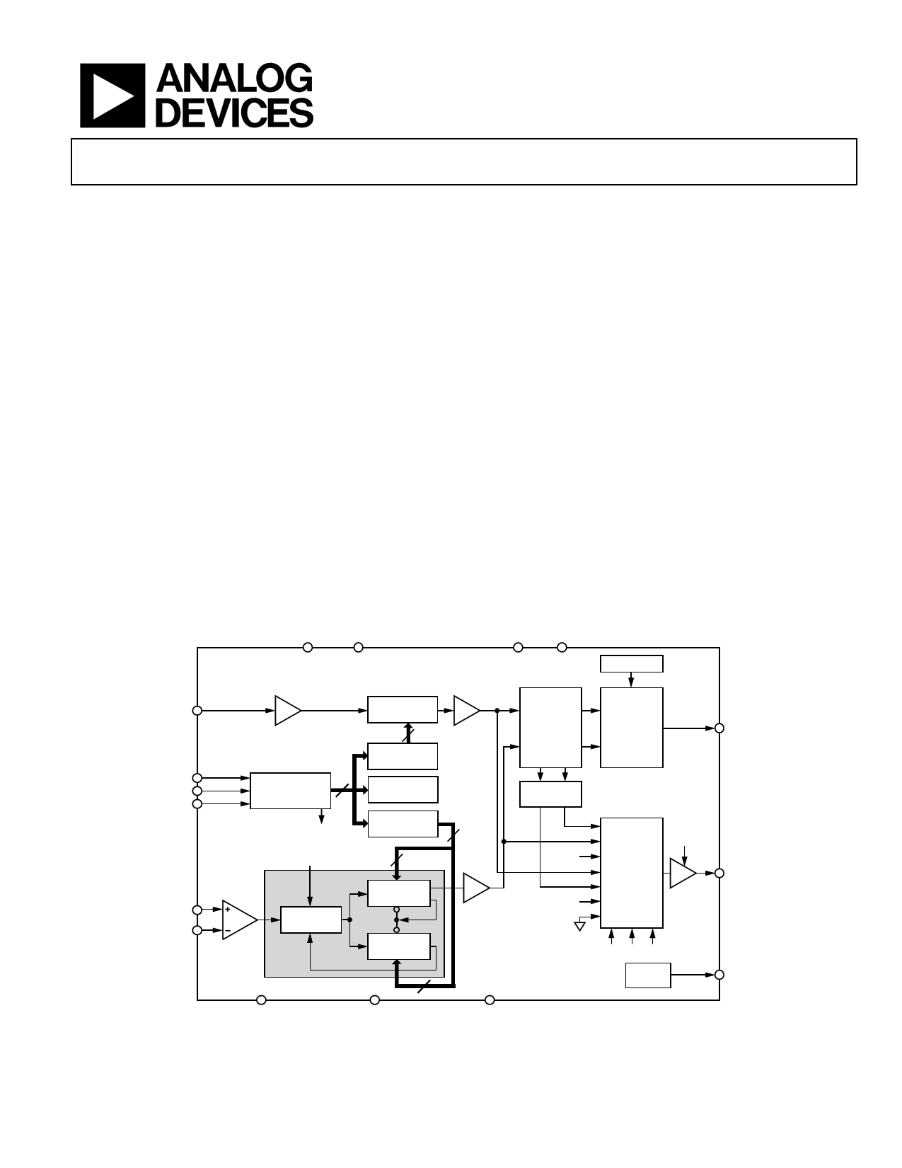
FUNCTIONAL BLOCK DIAGRAM
AVDD
DVDD
VP CPGND
ADF4116/ADF4117/ADF4118
REFERENCE
REFIN
CLK
DATA
LE
RFINA
RFINB
14-BIT
R COUNTER
14
R COUNTER
LATCH
21-BIT
INPUT REGISTER 19
FUNCTION
LATCH
SDOUT
FROM
FUNCTION LATCH
A, B COUNTER
LATCH
13
N = BP + A
13-BIT
B COUNTER
PRESCALER
P/P + 1
LOAD
LOAD
5-BIT
A COUNTER
18
PHASE
FREQUENCY
DETECTOR
LOCK
DETECT
AVDD
SDOUT
5
CE
AGND
DGND
Figure 1.
CHARGE
PUMP
MUX
HIGH Z
M3 M2 M1
FLO
SWITCH
CP
MUXOUT
FLO
Rev. D
Information furnished by Analog Devices is believed to be accurate and reliable. However, no
responsibility is assumed by Analog Devices for its use, nor for any infringements of patents or other
rights of third parties that may result from its use. Specifications subject to change without notice. No
license is granted by implication or otherwise under any patent or patent rights of Analog Devices.
Trademarksandregisteredtrademarksarethepropertyoftheirrespectiveowners.
One Technology Way, P.O. Box 9106, Norwood, MA 02062-9106, U.S.A.
Tel: 781.329.4700
www.analog.com
Fax: 781.461.3113 ©2000–2007 Analog Devices, Inc. All rights reserved.
1 page 
ADF4116/ADF4117/ADF4118
TIMING CHARACTERISTICS
AVDD = DVDD = 3 V ± 10%, 5 V ± 10%; AVDD ≤ VP < 6.0 V; AGND = DGND = CPGND = 0 V; TA = TMIN to TMAX, unless otherwise noted.
Guaranteed by design, but not production tested.
Table 2.
Parameter
t1
t2
t3
t4
t5
t6
Limit at TMIN to TMAX (B, Y Version)
10
10
25
25
10
20
Unit
ns min
ns min
ns min
ns min
ns min
ns min
Test Conditions/Comments
DATA to CLK setup time
DATA to CLK hold time
CLK high duration
CLK low duration
CLK to LE setup time
LE pulse width
CLK
DATA
DB20 (MSB)
t1 t2
DB19
LE
t3 t4
DB2
DB1
(CONTROL BIT C2)
LE
Figure 2. Timing Diagram
DB0 (LSB)
(CONTROL BIT C1)
t6
t5
Rev. D | Page 5 of 28
5 Page 
–60
VDD = 3V
VP = 5V
–70
–80
–90
–100 0
20 40 60 80
TEMPERATURE (°C)
100
Figure 22. ADF4118 Reference Spurs vs. Temperature
(836 MHz, 30 kHz, 3 kHz)
3.0
2.5
2.0
1.5
1.0
0.5
0 0 50 100 150
PRESCALER OUTPUT FREQUENCY (MHz)
Figure 23. DIDD vs. Prescaler Output Frequency
200
ADF4116/ADF4117/ADF4118
1.2
1.0
0.8
0.6
0.4
0.2
0
–0.2
–0.4
–0.6
–0.8
–1.0
–1.2
0
VP = 5V
ICP SETTING: 1mA
0.5 1.0 1.5 2.0 2.5 3.0 3.5 4.0 4.5
VCP (V)
5.0
Figure 24. Charge Pump Output Characteristics
Rev. D | Page 11 of 28
11 Page | ||
| Páginas | Total 28 Páginas | |
| PDF Descargar | [ Datasheet ADF4117.PDF ] | |
Hoja de datos destacado
| Número de pieza | Descripción | Fabricantes |
| ADF4110 | RF PLL Frequency Synthesizers | Analog Devices |
| ADF4111 | RF PLL Frequency Synthesizers | Analog Devices |
| ADF4112 | RF PLL Frequency Synthesizers | Analog Devices |
| ADF4113 | RF PLL Frequency Synthesizers | Analog Devices |
| Número de pieza | Descripción | Fabricantes |
| SLA6805M | High Voltage 3 phase Motor Driver IC. |
Sanken |
| SDC1742 | 12- and 14-Bit Hybrid Synchro / Resolver-to-Digital Converters. |
Analog Devices |
|
DataSheet.es es una pagina web que funciona como un repositorio de manuales o hoja de datos de muchos de los productos más populares, |
| DataSheet.es | 2020 | Privacy Policy | Contacto | Buscar |