|
|
|
PDF CD40193BMS Data sheet ( Hoja de datos )
| Número de pieza | CD40193BMS | |
| Descripción | CMOS Presettable Up/Down Counters (Dual Clock With Reset) | |
| Fabricantes | Intersil Corporation | |
| Logotipo | ||
Hay una vista previa y un enlace de descarga de CD40193BMS (archivo pdf) en la parte inferior de esta página. Total 12 Páginas | ||
|
No Preview Available !
December 1992
CD40192BMS
CD40193BMS
CMOS Presettable Up/Down Counters
(Dual Clock With Reset)
Features
Description
• CD40192BMS - BCD Type
• CD40193BMS - Binary Type
• High Voltage Type (20V Rating)
• Individual Clock Lines for Counting Up or Counting
Down
• Synchronous High-Speed Carry and Borrow Propaga-
tion Delays for Cascading
• Asynchronous Reset and Preset Capability
• Medium Speed Operation
- fCL = 8MHz (typ.) at 10V
• 5V, 10V and 15V Parametric Ratings
• Standardize Symmetrical Output Characteristics
• 100% Tested for Quiescent Current at 20V
• Maximum Input Current of 1µA at 18V Over Full Pack-
age Temperature Range; 100nA at 18V and +25oC
• Noise Margin (Over Full Package/Temperature Range)
- 1V at VDD = 5V
- 2V at VDD = 10V
- 2.5V at VDD = 15V
• Meets All Requirements of JEDEC Tentative Standard
No. 13B, “Standard Specifications for Description of
‘B’ Series CMOS Devices”
Applications
• Up/Down Difference Counting
• Multistage Ripple Counting
• Synchronous Frequency Dividers
• A/D and D/A Conversion
• Programmable Binary or BCD Counting
CD40192BMS Presettable BCD Up/Down Counter and the
CD40193BMS Presettable Binary Up/Down Counter each con-
sist of 4 synchronously clocked, gated “D” type flip-flops con-
nected as a counter. The inputs consist of 4 individual jam lines,
a PRESET ENABLE control, individual CLOCK UP and
CLOCK DOWN signals and a master RESET. Four buffered Q
signal outputs as well as CARRY and BORROW outputs for
multiple-stage counting schemes are provided.
The counter is cleared so that all outputs are in a low state by a
high on the RESET line. A RESET is accomplished asynchro-
nously with the clock. Each output is individually programmable
asynchronously with the clock to the level on the corresponding
jam input when the PRESET ENABLE control is low.
The counter counts up one count on the positive clock edge of
the CLOCK UP signal provided the CLOCK DOWN line is high.
The counter counts down one count on the positive clock edge
of the CLOCK DOWN signal provided the CLOCK UP line is
high.
The CARRY and BORROW signals are high when the counter
is counting up or down. The CARRY signal goes low one-half
clock cycle after the counter reaches its maximum count in the
count-up mode. The BORROW signal goes low one-half clock
cycle after the counter reaches its minimum count in the count-
down mode. Cascading of multiple packages is easily accom-
plished without the need for additional external circuitry by tying
the BORROW and CARRY outputs to the CLOCK DOWN and
CLOCK UP inputs, respectively, of the succeeding counter
package.
The CD40192BMS and CD40193BMS are supplied in these
16-lead outline packages:
Braze Seal DIP
Frit Seal DIP
Ceramic Flatpack
* CD40192B Only
*H4W, †H4X
H1F
*H6P, †H6W
†CD40193B Only
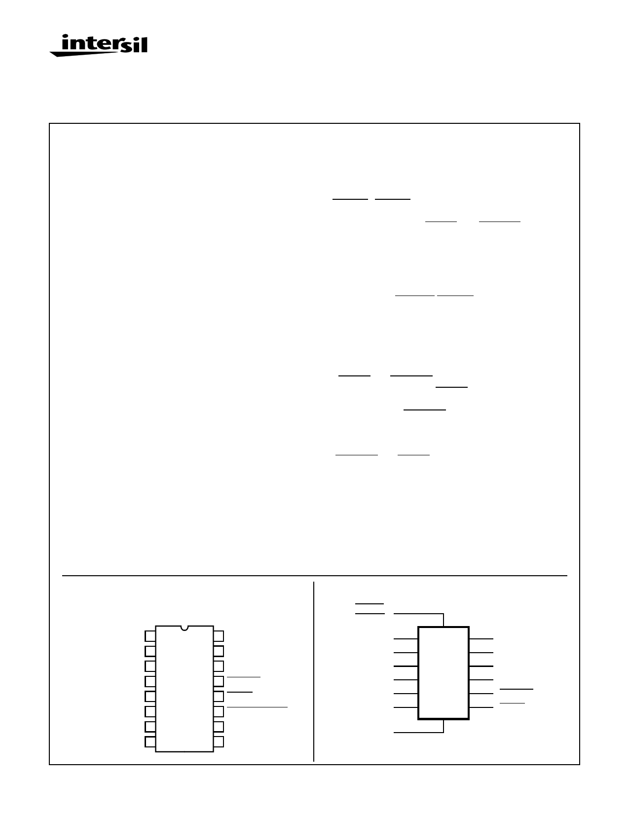
Pinout
CD40192BMS, CD40193BMS
TOP VIEW
J2 1
Q2 2
Q1 3
CLOCK DOWN 4
CLOCK UP 5
Q3 6
Q4 7
VSS 8
16 VDD
15 J1
14 RESET
13 BORROW
12 CARRY
11 PRESET ENABLE
10 J3
9 J4
Functional Diagram
PRESET
ENABLE
J1
J2
J3
J4
CLOCK UP
CLOCK DOWN
15
1
10
9
5
4
RESET
11
3
2
6
7
13
12
Q1
Q2
Q3
Q4
BORROW
CARRY
14 VDD = 16
VSS = 8
CAUTION: These devices are sensitive to electrostatic discharge; follow proper IC Handling Procedures.
1-888-INTERSIL or 321-724-7143 | Copyright © Intersil Corporation 1999
7-1419
File Number 3363
1 page 
Specifications CD40192BMS, CD40193BMS
TABLE 3. ELECTRICAL PERFORMANCE CHARACTERISTICS (Continued)
LIMITS
PARAMETER
Minimum Clock Pulse
Width
Input Capacitance
Input Capacitance
SYMBOL
CONDITIONS
TW VDD = 5V
VDD = 10V
VDD = 15V
CIN Reset
CIN All Other Inputs
NOTES
1, 2, 3
1, 2, 3
1, 2, 3
1, 2
1, 2
TEMPERATURE
+25oC
+25oC
+25oC
+25oC
+25oC
MIN
-
-
-
-
-
MAX
180
90
60
15
7.5
UNITS
ns
ns
ns
pF
pF
NOTES:
1. All voltages referenced to device GND.
2. The parameters listed on Table 3 are controlled via design or process and are not directly tested. These parameters are characterized on
initial design release and upon design changes which would affect these characteristics.
3. CL = 50pF, RL = 200K, Input TR, TF < 20ns.
4. If more than one unit is cascaded, TRCL should be made less than or equal to the sumof the transition time and the fixed propagation
delay of the output of the driving stage for the estimated capacitive load.
5. The time required for RESET or PRESET ENABLE control to be removed before clocking. See timing diagram defining TREM.
TABLE 4. POST IRRADIATION ELECTRICAL PERFORMANCE CHARACTERISTICS
LIMITS
PARAMETER
Supply Current
N Threshold Voltage
N Threshold Voltage
Delta
P Threshold Voltage
P Threshold Voltage
Delta
Functional
Propagation Delay Time
SYMBOL
CONDITIONS
IDD VDD = 20V, VIN = VDD or GND
VNTH VDD = 10V, ISS = -10µA
∆VTN VDD = 10V, ISS = -10µA
VTP
∆VTP
VSS = 0V, IDD = 10µA
VSS = 0V, IDD = 10µA
F
TPHL
TPLH
VDD = 18V, VIN = VDD or GND
VDD = 3V, VIN = VDD or GND
VDD = 5V
NOTES: 1. All voltages referenced to device GND.
2. CL = 50pF, RL = 200K, Input TR, TF < 20ns.
NOTES
1, 4
1, 4
1, 4
TEMPERATURE
+25oC
+25oC
+25oC
MIN
-
-2.8
-
1, 4
+25oC
0.2
1, 4
+25oC
-
1
1, 2, 3, 4
+25oC
+25oC
VOH >
VDD/2
-
3. See Table 2 for +25oC limit.
4. Read and Record
MAX
25
-0.2
±1
2.8
±1
VOL <
VDD/2
1.35 x
+25oC
Limit
UNITS
µA
V
V
V
V
V
ns
TABLE 5. BURN-IN AND LIFE TEST DELTA PARAMETERS +25oC
PARAMETER
SYMBOL
DELTA LIMIT
Supply Current - MSI-2
Output Current (Sink)
Output Current (Source)
IDD
IOL5
IOH5A
± 1.0µA
± 20% x Pre-Test Reading
± 20% x Pre-Test Reading
7-1423
5 Page 
CD40192BMS, CD40193BMS
RESET
1
0
PE
J1
J2
J3
J4
CLK
UP
CLK
DN
1
0
1
0
1
0
1
0
1
0
1
0
1
0
Q1 1
0
Q2 1
0
Q3 1
0
Q4 1
0
CARRY
1
0
BORROW
1
0
COUNT
0 7 890 1 2 1 0 98 7
FIGURE 11. CD40192BMS TIMING DIAGRAM
RESET
PE
J1
1
0
1
0
1
0
J2
1
0
J3
1
0
J4
1
0
CLK 1
UP 0
CLK 1
DN 0
Q1
1
0
Q2
1
0
Q3
1
0
Q4
1
0
CARRY
1
0
BORROW
1
0
COUNT
0 13 14 15 0 1 2 1 0 15 14 13
FIGURE 12. CD40193BMS TIMING DIAGRAM
CLOCK
RESET
PRESET ENABLE
tWH
tWL
trem*
*RESET OR PRESET ENABLE
REMOVAL TIME
FIGURE 13. TIMING DIAGRAM DEFINING trem
J1 J2 J3 J4
CLOCK UP
CLOCK DOWN
CD40192BMS
OR
CD40193BMS
RESET
PRESET
ENABLE
Q1 Q2 Q3 Q4
CARRY
BORROW
J1 J2 J3 J4
CLOCK UP
CLOCK DOWN
CD40192BMS
OR
CD40193BMS
Q1 Q2 Q3 Q4
CARRY
BORROW
FIGURE 14. CASCADED COUNTER PACKAGES
7-1429
11 Page | ||
| Páginas | Total 12 Páginas | |
| PDF Descargar | [ Datasheet CD40193BMS.PDF ] | |
Hoja de datos destacado
| Número de pieza | Descripción | Fabricantes |
| CD40193BM | 4-Bit Up/Down Binary Counter | National Semiconductor |
| CD40193BMS | CMOS Presettable Up/Down Counters (Dual Clock With Reset) | Intersil Corporation |
| Número de pieza | Descripción | Fabricantes |
| SLA6805M | High Voltage 3 phase Motor Driver IC. |
Sanken |
| SDC1742 | 12- and 14-Bit Hybrid Synchro / Resolver-to-Digital Converters. |
Analog Devices |
|
DataSheet.es es una pagina web que funciona como un repositorio de manuales o hoja de datos de muchos de los productos más populares, |
| DataSheet.es | 2020 | Privacy Policy | Contacto | Buscar |