|
|
|
PDF HI-3588 Data sheet ( Hoja de datos )
| Número de pieza | HI-3588 | |
| Descripción | Receiver | |
| Fabricantes | HOLTIC | |
| Logotipo | ||
Hay una vista previa y un enlace de descarga de HI-3588 (archivo pdf) en la parte inferior de esta página. Total 13 Páginas | ||
|
No Preview Available !
July 2012
HI-3588
ARINC 429
Receiver with SPI Interface
GENERAL DESCRIPTION
The HI-3588 from Holt Integrated Circuits is a silicon gate
CMOS device for interfacing a Serial Peripheral Interface
(SPI) enabled microcontroller to an ARINC 429 serial bus.
The device provides one receiver with user-programmable
label recognition for any combination of 256 possible
labels, a 32 by 32 Receive FIFO and an analog line
receiver. Receive FIFO status can be monitored using the
programmable external interrupt pin, or by polling the
HI-3588 Status Register. Other features include the ability
to switch the bit-signifiance of ARINC 429 labels. The
ARINC input pins are available with different input resis-
tance values to provide flexibility when adding external
lightning protection circuitry.
The Serial Peripheral Interface minimizes the number of
host interface signals allowing for a small footprint device
which can be interfaced to a wide variety of industry-
standard microcontrollers supporting SPI. Alternatively,
the SPI signals may be controlled using just four general
purpose I/O port pins from a microcontroller or custom
FPGA. The SPI and all control signals are CMOS and TTL
compatible and support 3.3V or 5V operation.
The HI-3588 checks received data against ARINC 429
electrical, timing and protocol requirements. ARINC 429
databus timing comes from a 1 MHz clock input,
or an internal counter can derive it from higher clock
frequencies having certain fixed values, possibly the
external host processor clock.
FEATURES
· ARINC specification 429 compliant
· 3.3V or 5.0V logic supply operation
· On-chip analog line receiver connects directly to
ARINC 429 bus
· Programmable label recognition for 256 labels
· 32 x 32 Receive Data FIFO
· Programmable data rate selection
· High-speed, four-wire Serial Peripheral Interface
· Label bit-order control
· Parity checking may be disabled to allow 32-bit data
reception
· Low power
· Industrial & extended temperature ranges
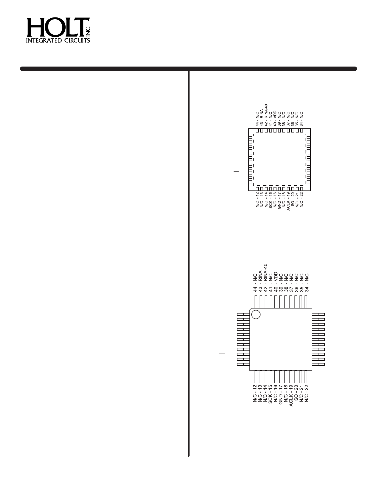
PIN CONFIGURATIONS (Top View)
N/C - 1
RINB-40 - 2
RINB - 3
N/C - 4
N/C - 5
N/C - 6
MR - 7
SI - 8
CS - 9
N/C - 10
N/C - 11
HI-3588PCI
HI-3588PCT
33 - N/C
32 - N/C
31 - N/C
30 - GND
29 - N/C
28 - N/C
27 - N/C
26 - N/C
25 - RFLAG
24 - N/C
23 - N/C
44 - Pin Plastic 7mm x 7mm
Chip-Scale Package (QFN)
N/C - 1
RINB-40 - 2
RINB - 3
N/C - 4
N/C - 5
N/C - 6
MR - 7
SI - 8
CS - 9
N/C - 10
N/C - 11
HI-3588PQI
HI-3588PQT
33 - N/C
32 - N/C
31 - N/C
30 - GND
29 - N/C
28 - N/C
27 - N/C
26 - N/C
25 - RFLAG
24 - N/C
23 - N/C
44 - Pin Plastic Quad Flat Pack (PQFP)
(DS3588 Rev. G)
HOLT INTEGRATED CIRCUITS
www.holtic.com
07/12
1 page 
HI-3588
FUNCTIONAL DESCRIPTION (cont.)
ARINC 429 RECEIVER
ARINC BUS INTERFACE
Figure 1 shows the input circuit for the ARINC 429 line receiver. The
ARINC 429 specification requires the following detection levels:
STATE
ONE
NULL
ZERO
DIFFERENTIAL VOLTAGE
+6.5 Volts to +13 Volts
+2.5 Volts to -2.5 Volts
-6.5 Volts to -13 Volts
RINA-40
RINA
VDD
DIFFERENTIAL
AMPLIFIERS
COMPARATORS
ONE
RINB
RINB-40
GND
VDD
GND
FIGURE 1. ARINC RECEIVER INPUT
NULL
ZERO
The HI-3588 guarantees recognition of these levels with a common
mode voltage with respect to GND less than ±30V for the worst case
condition (3.15V supply and 13V signal level). Design tolerances
guarantee detection of the above levels, so the actual acceptance
ranges are slightly larger. If the ARINC signal (including nulls) is
outside the differential voltage ranges, the HI-3588 receiver rejects
the data.
RECEIVER LOGIC OPERATION
Figure 2 is a block diagram showing receiver logic.
BIT TIMING
The ARINC 429 specification defines the following timing toler-
ances for received data:
The HI-3588 accepts signals within these tolerances and rejects
signals outside these tolerances. Receiver logic achieves this as
described below:
1. An accurate 1MHz clock source is required to validate the
receive signal timing. Less than 1% error is recommended.
2. The receiver uses three separate 10-bit sampling shift reg-
isters for Ones detection, Zeros detection and Null detection.
When the input signal is within the differential voltage range
for any shift register’s state (One Zero or Null) sampling
clocks a high bit into that register. When the receive signal is
outside the differential voltage range defined for any shift reg-
ister, a low bit is clocked. Only one shift register can clock a
high bit for any given sample. All three registers clock low
bits if the differential input voltage is between defined state
voltage bands.
Valid data bits require at least three consecutive One or Zero
samples (three high bits) in the upper half of the Ones or Ze-
ros sampling shift register, and at least three consecutive Null
samples (three high bits) in the lower half of the Null sampling
shift register within the data bit interval.
A word gap Null requires at least three consecutive Null sam-
ples (three high bits) in the upper half of the Null sampling
shift register and at least three consecutive Null samples
(three high bits) in the lower half of the Null sampling shift reg-
ister. This guarantees the minimum pulse width.
3. To validate the receive data bit rate, each bit must follow
its preceding bit by not less than 8 samples and not more
than 12 samples. With exactly 1MHz input clock frequency,
the acceptable data bit rates are:
DATA BIT RATE MIN
DATA BIT RATE MAX
HIGH SPEED LOW SPEED
83K BPS
125K BPS
10.4K BPS
15.6K BPS
4. Following the last data bit of a valid reception, the Word
Gap timer samples the Null shift register every 10 input
clocks (every 80 clocks for low speed). If a Null is present,
the Word Gap counter is incremented. A Word Gap count of 3
enables the next reception.
BIT RATE
PULSE RISE TIME
PULSE FALL TIME
PULSE WIDTH
HIGH SPEED
100K BPS ± 1%
1.5 ± 0.5 µsec
1.5 ± 0.5 µsec
5 µsec ± 5%
LOW SPEED
12K -14.5K BPS
10 ± 5 µsec
10 ± 5 µsec
34.5 to 41.7 µsec
HOLT INTEGRATED CIRCUITS
5
5 Page 
HI-3588
ORDERING INFORMATION
HI - 3588 xx x x
PART
NUMBER
Blank
F
PART
NUMBER
I
T
PART
NUMBER
PC
PQ
LEAD
FINISH
Tin / Lead (Sn / Pb) Solder
100% Matte Tin (Pb-free, RoHS compliant)
TEMPERATURE
RANGE
-40°C TO +85°C
-55°C TO +125°C
FLOW
I
T
BURN
IN
No
No
PACKAGE
DESCRIPTION
44 PIN PLASTIC CHIP-SCALE, QFN (44PCS)
44 PIN PLASTIC QUAD FLAT PACK, PQFP (44PMQS)
HOLT INTEGRATED CIRCUITS
11
11 Page | ||
| Páginas | Total 13 Páginas | |
| PDF Descargar | [ Datasheet HI-3588.PDF ] | |
Hoja de datos destacado
| Número de pieza | Descripción | Fabricantes |
| HI-3582 | 3.3V Terminal IC | HOLTIC |
| HI-3582A | 3.3V Terminal IC | HOLTIC |
| HI-3583 | 3.3V Terminal IC | HOLTIC |
| HI-3583A | 3.3V Terminal IC | HOLTIC |
| Número de pieza | Descripción | Fabricantes |
| SLA6805M | High Voltage 3 phase Motor Driver IC. |
Sanken |
| SDC1742 | 12- and 14-Bit Hybrid Synchro / Resolver-to-Digital Converters. |
Analog Devices |
|
DataSheet.es es una pagina web que funciona como un repositorio de manuales o hoja de datos de muchos de los productos más populares, |
| DataSheet.es | 2020 | Privacy Policy | Contacto | Buscar |