|
|
|
PDF AD1585 Data sheet ( Hoja de datos )
| Número de pieza | AD1585 | |
| Descripción | Precision Series Mode Voltage References | |
| Fabricantes | Analog Devices | |
| Logotipo | ||
Hay una vista previa y un enlace de descarga de AD1585 (archivo pdf) en la parte inferior de esta página. Total 16 Páginas | ||
|
No Preview Available !
Data Sheet
2.5 V to 5.0 V Micropower, Precision
Series Mode Voltage References
AD1582/AD1583/AD1584/AD1585
FEATURES
Series reference (2.5 V, 3 V, 4.096 V, 5 V)
Low quiescent current: 70 µA maximum
Current output capability: ±5 mA
Wide supply range: VIN = VOUT + 200 mV to 12 V
Wideband noise (10 Hz to 10 kHz): 50 µV rms
Specified temperature range: −40°C to +125°C
Compact, surface-mount SOT-23 package
APPLICATIONS
Portable, battery-powered equipment; for example,
notebook computers, cellular phones, pagers, PDAs, GPSs,
and DMMs
Computer workstations; suitable for use with a wide range
of video RAMDACs
Smart industrial transmitters
PCMCIA cards
Automotive
Hard disk drives
3 V/5 V, 8-bit/12-bit data converters
GENERAL DESCRIPTION
The AD1582/AD1583/AD1584/AD1585 are low cost, low power,
low dropout, precision band gap references. These designs are
available as 3-terminal (series) devices and are packaged in the
compact SOT-23, 3-lead surface-mount package. The versatility
of these references makes them ideal for use in battery-powered
3 V or 5 V systems where there can be wide variations in supply
voltage and a need to minimize power dissipation.
The superior accuracy and temperature stability of the AD1582/
AD1583/AD1584/AD1585 result from the precise matching and
thermal tracking of on-chip components. Patented temperature
drift curvature correction design techniques minimize the
nonlinearities in the voltage output temperature characteristic.
PIN CONFIGURATION
VOUT 1
AD1582/
AD1583/
AD1584/
AD1585
3 VIN
GND 2 TOP VIEW
(Not to Scale)
Figure 1. 3-Lead SOT-23-3 (RT Suffix)
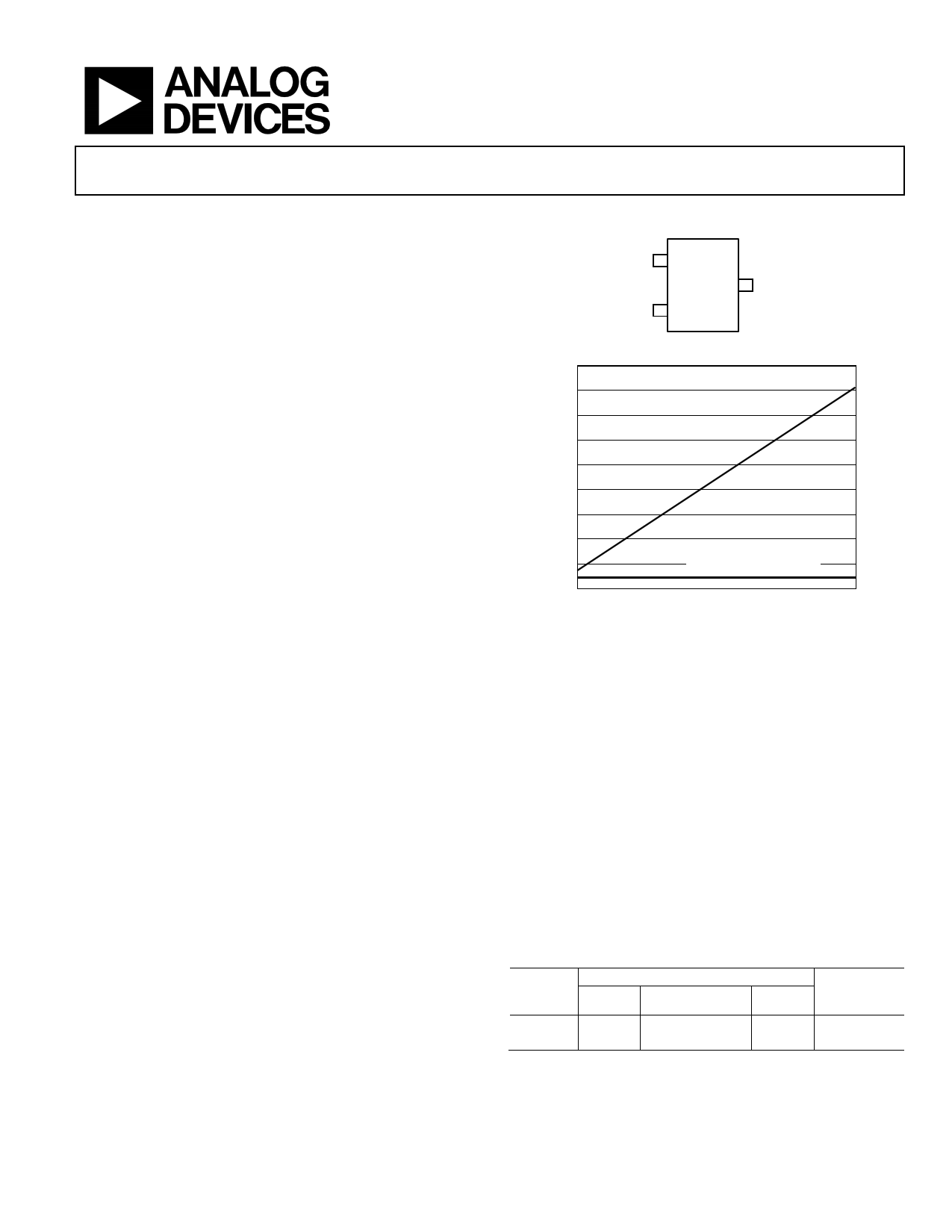
900
800
700
600
SHUNT REFERENCE1
500
400
300
200
100 AD1582 SERIES REFERENCE
0
2.7
VSUPPLY (V)
5
13.076kΩ SOURCE RESISTOR.
Figure 2. Supply Current (μA) vs. Supply Voltage (V)
The AD1582/AD1583/AD1584/AD1585 series mode devices
source or sink up to 5 mA of load current and operate efficiently
with only 200 mV of required headroom supply. These parts
draw a maximum 70 μA of quiescent current with only a
1.0 μA/V variation with supply voltage. The advantage of
these designs over conventional shunt devices is extraordinary.
Valuable supply current is no longer wasted through an input
series resistor, and maximum power efficiency is achieved at
all input voltage levels.
The AD1582/AD1583/AD1584/AD1585 are available in two
grades, A and B, and are provided in a tiny footprint, the SOT-
23. All grades are specified over the industrial temperature
range of −40°C to +125°C.
Table 1. AD158x Products, Three Electrical Grades
Electrical
Grade
AD1582
Initial Accuracy
AD1583/AD1585
AD1584
Temperature
Coefficient
(ppm°C)
B 0.08% 0.10%
0.10% 50
A 0.80% 1.00%
0.98% 100
Rev. J
Document Feedback
Information furnished by Analog Devices is believed to be accurate and reliable. However, no
responsibility is assumed by Analog Devices for its use, nor for any infringements of patents or other
rights of third parties that may result from its use. Specifications subject to change without notice. No
license is granted by implication or otherwise under any patent or patent rights of Analog Devices.
Trademarksandregisteredtrademarksarethepropertyoftheirrespectiveowners.
One Technology Way, P.O. Box 9106, Norwood, MA 02062-9106, U.S.A.
Tel: 781.329.4700 ©1997–2013 Analog Devices, Inc. All rights reserved.
Technical Support
www.analog.com
1 page 
Data Sheet
AD1584 SPECIFICATIONS
TA = TMIN to TMAX, VIN = 5 V, unless otherwise noted.
Table 4.
Parameter
OUTPUT VOLTAGE (@ 25°C)
VO
INITIAL ACCURACY ERROR (@ 25°C)
VOERR
OUTPUT VOLTAGE TEMPERATURE DRIFT
TEMPERATURE COEFFICIENT (TCVO)
−40°C < TA < +125°C
0°C < TA < 70°C
MINIMUM SUPPLY HEADROOM (VIN – VOUT)
LOAD REGULATION
0 mA < IOUT < 5 mA (−40°C to +85°C)
0 mA < IOUT < 5 mA (−40°C to +125°C)
−5 mA < IOUT < 0 mA (−40°C to +85°C)
−5 mA < IOUT < 0 mA (−40°C to +125°C)
−0.1 mA < IOUT < +0.1 mA (−40°C to +85°C)
−0.1 mA < IOUT < +0.1 mA (−40°C to +125°C)
LINE REGULATION
VOUT + 200 mV < VIN 12 V
IOUT = 0 mA
RIPPLE REJECTION (ΔVOUT/ΔVIN)
VIN = 5 V ± 100 mV (f = 120 Hz)
QUIESCENT CURRENT
SHORT-CIRCUIT CURRENT TO GROUND
NOISE VOLTAGE (@ 25°C)
0.1 Hz to 10 Hz
10 Hz to 10 kHz
TURN-ON SETTLING TIME TO 0.1%
CL = 0.2 µF
LONG-TERM STABILITY
1000 Hours @ 25°C
OUTPUT VOLTAGE HYSTERESIS
TEMPERATURE RANGE
Specified Performance (A, B, C)
Operating Performance (A, B, C)
AD1582/AD1583/AD1584/AD1585
AD1584A
Min Typ Max
AD1584B
Min Typ Max
Unit
4.056 4.096 4.136 4.092 4.096 4.100 V
−40
−0.98
+40
+0.98
100
−4
−0.1
+4 mV
+0.1 %
50 ppm/°C
40 100
18 50 ppm/°C
35 15 ppm/°C
200 200 mV
0.32 0.32 mV/mA
0.52 0.52 mV/mA
0.40 0.40 mV/mA
0.6 0.6 mV/mA
3.2 3.2 mV/mA
4.1 4.1 mV/mA
80
110
90
100
115
−40
−55
25
70
15
140
+125
−125
80
−40
−55
110
90
100
115
25
70
15
140
+125
+125
µV/V
dB
µA
mA
µV p-p
µV rms
µs
ppm/1000 hr
ppm
°C
°C
Rev. J | Page 5 of 16
5 Page 
Data Sheet
APPLICATIONS INFORMATION
The AD1582/AD1583/AD1584/AD1585 are series references
that can be used for many applications. To achieve optimum
performance with these references, only two external compo-
nents are required. Figure 10 shows the AD1582/AD1583/
AD1584/AD1585 configured for operation under all loading
conditions. With a simple 4.7 µF capacitor attached to the input
and a 1 µF capacitor applied to the output, the devices can achieve
specified performance for all input voltage and output current
requirements. For best transient response, add a 0.1 µF capacitor
in parallel with the 4.7 µF capacitor. While a 1 µF output capacitor
can provide stable performance for all loading conditions, the
AD1582/AD1583/AD1584/AD1585 can operate under low
(−100 µA < IOUT < +100 µA) current conditions with just a
0.2 µF output capacitor. The 4.7 µF capacitor on the input can
be reduced to 1 μF in this condition.
Unlike conventional shunt reference designs, the AD1582/
AD1583/AD1584/AD1585 provide stable output voltages at
constant operating current levels. When properly decoupled,
as shown in Figure 10, these devices can be applied to any
circuit and provide superior low power solutions.
+
VOUT
–
1
1µF
2
AD1582/
AD1583/
AD1584/
AD1585
3
VIN
4.7µF
Figure 10. Typical Connection Diagram
TEMPERATURE PERFORMANCE
The AD1582/AD1583/AD1584/AD1585 are designed for
applications where temperature performance is important.
Extensive temperature testing and characterization ensure
that device performance is maintained over the specified
temperature range.
The error band guaranteed with the AD1582/AD1583/AD1584/
AD1585 is the maximum deviation from the initial value at 25°C.
Therefore, for a given grade of the AD1582/AD1583/AD1584/
AD1585, the designer can easily determine the maximum total
error by summing initial accuracy and temperature variation. For
example, for the AD1582BRT, the initial tolerance is ±2 mV, and
the temperature error band is ±8 mV; therefore, the reference is
guaranteed to be 2.5 V ± 10 mV from −40°C to +125°C.
Figure 11 shows the typical output voltage drift for the AD1582/
AD1583/AD1584/AD1585 and illustrates the methodology. The
box in Figure 11 is bounded on the x-axis by operating tempera-
ture extremes. It is bounded on the y-axis by the maximum
and minimum output voltages observed over the operating
temperature range. The slope of the diagonal drawn from the
initial output value at 25°C to the output values at +125°C and
−40°C determines the performance grade of the device.
AD1582/AD1583/AD1584/AD1585
Duplication of these results requires a test system that is highly
accurate with stable temperature control. Evaluation of the
AD1582/AD1583/AD1584/AD1585 produces curves similar
to those in Figure 5 and Figure 11, but output readings can vary
depending on the test methods and test equipment used.
2.504
2.502
2.500
2.498
2.496
2.494
2.492
–40
–20 0
20 40 60 80 100
TEMPERATURE (°C)
Figure 11. Output Voltage vs. Temperature
120
VOLTAGE OUTPUT NONLINEARITY VS.
TEMPERATURE
When using a voltage reference with data converters, it is
important to understand the impact that temperature drift can
have on converter performance. The nonlinearity of the reference
output drift represents additional error that cannot be easily
calibrated out of the overall system. To better understand the
impact such a drift can have on a data converter, refer to Figure 12,
where the measured drift characteristic is normalized to the
endpoint average drift. The residual drift error for the AD1582/
AD1583/AD1584/AD1585 of approximately 200 ppm demon-
strates that these parts are compatible with systems that require
12-bit accurate temperature performance.
250
200
150
100
50
0
–50
–50
–25 0
25 50
TEMPERATURE (°C)
Figure 12. Residual Drift Error
75
100
Rev. J | Page 11 of 16
11 Page | ||
| Páginas | Total 16 Páginas | |
| PDF Descargar | [ Datasheet AD1585.PDF ] | |
Hoja de datos destacado
| Número de pieza | Descripción | Fabricantes |
| AD1580 | Precision Shunt Voltage Reference | Analog Devices |
| AD1582 | Precision Series Mode Voltage References | Analog Devices |
| AD1583 | Precision Series Mode Voltage References | Analog Devices |
| AD1584 | Precision Series Mode Voltage References | Analog Devices |
| Número de pieza | Descripción | Fabricantes |
| SLA6805M | High Voltage 3 phase Motor Driver IC. |
Sanken |
| SDC1742 | 12- and 14-Bit Hybrid Synchro / Resolver-to-Digital Converters. |
Analog Devices |
|
DataSheet.es es una pagina web que funciona como un repositorio de manuales o hoja de datos de muchos de los productos más populares, |
| DataSheet.es | 2020 | Privacy Policy | Contacto | Buscar |