|
|
|
PDF ICS932S422C Data sheet ( Hoja de datos )
| Número de pieza | ICS932S422C | |
| Descripción | PCIe Gen 2 main Clock | |
| Fabricantes | Integrated Circuit Systems | |
| Logotipo | ||
Hay una vista previa y un enlace de descarga de ICS932S422C (archivo pdf) en la parte inferior de esta página. Total 21 Páginas | ||
|
No Preview Available !
Integrated
Circuit
Systems, Inc.
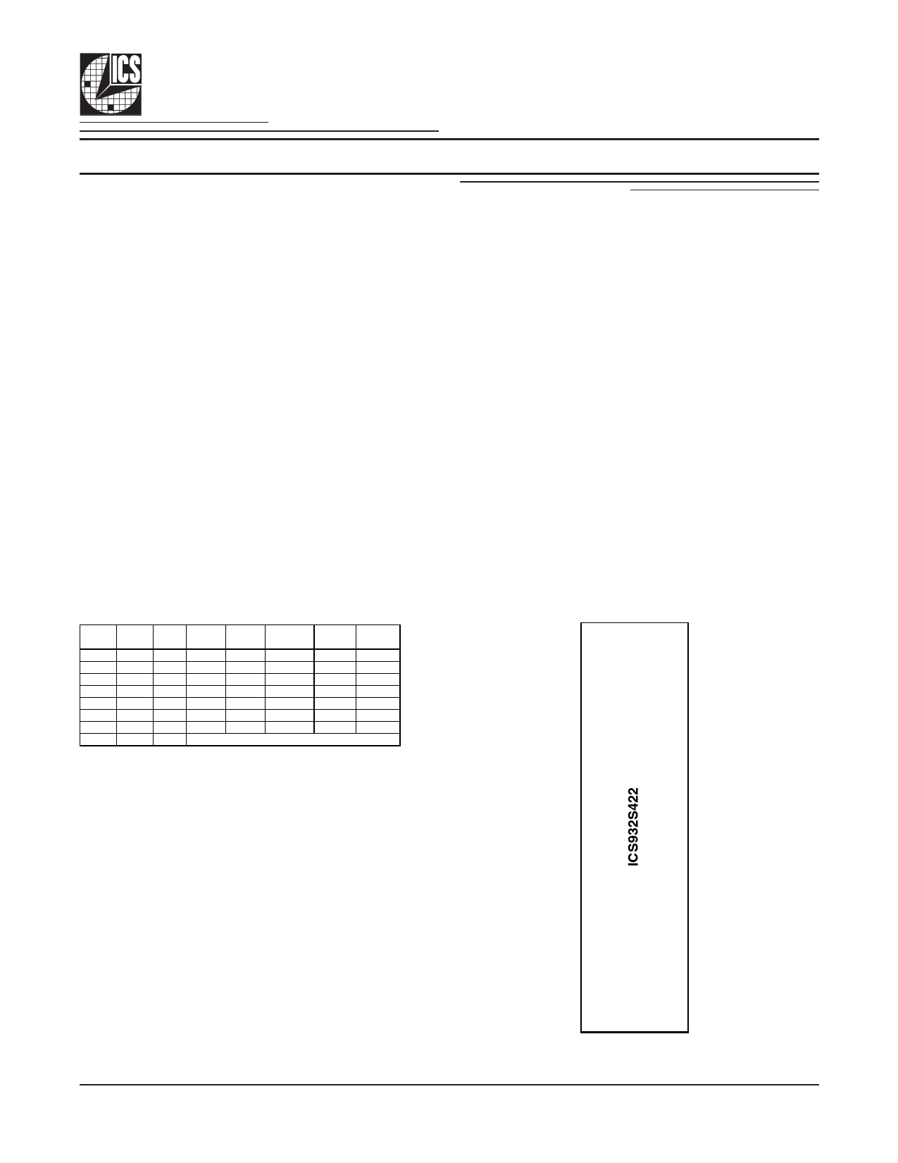
ICS932S422C
PCIe Gen 2 main Clock for Intel-based Servers
Recommended Application:
PCIe Gen 2 & FBD compliant CK410B/CK410B+ clock for
Intel-based servers
Output Features:
• 5 - 0.7V current-mode differential CPU pairs
• 4 - 0.7V current-mode differential SRC pair
• 4 - PCI (33MHz)
• 3 - PCICLK_F, (33MHz) free-running
• 1 - 48MHz
• 2 - REF, 14.318MHz
Key Specifications:
• CPU cycle-cycle jitter: < 50ps
• SRC cycle-cycle jitter: < 125ps
• PCI cycle-cycle jitter: < 500ps
• CPU output skew: < 100ps
• SRC output skew: < 250ps
• ± 300ppm frequency accuracy on all outputs except
48MHz
• ± 100ppm frequency accuracy on 48MHz
Features/Benefits:
• Supports spread spectrum modulation, 0 to -0.5%
down spread
• Uses external 14.318MHz crystal and external load
capacitors for low ppm synthesis error
• CPU clocks independent of SRC/PCI clocks
• D2/D3 SMBus address
• Compliant with PCIe Gen II phase noise specifications
Functionality
FSLC1
0
0
0
0
1
1
1
1
FSLB1
0
0
1
1
0
0
1
1
FSLA2
0
1
0
1
0
1
0
1
CPU
MHz
266.67
133.33
200.00
166.67
333.33
100.00
400.00
SRC
MHz
100.00
100.00
100.00
100.00
100.00
100.00
100.00
PCI
MHz
33.33
33.33
33.33
33.33
33.33
33.33
33.33
Reserved
REF
MHz
14.318
14.318
14.318
14.318
14.318
14.318
14.318
USB
MHz
48.000
48.000
48.000
48.000
48.000
48.000
48.000
1. FSLB and FSLC are three-level inputs. Please see VIL_FS and VIH_FS
specifications in the Input/Supply/Common Output Parameters Table for
correct values. Also refer to the Test Clarification Table.
2.FSLA is a low-threshold input. Please see the VIL_FS and VIH_FS
specifications in the Input/Supply/Common Output Parameters Table for correct values.
1412A—12/10/07
Pin Configuration
VDDPCI 1
GNDPCI 2
PCICLK0 3
PCICLK1 4
PCICLK2 5
PCICLK3 6
GNDPCI 7
VDDPCI 8
PCICLK_F0 9
PCICLK_F1 10
PCICLK_F2 11
VDD48 12
48MHz 13
GND48 14
VDDSRC 15
NC 16
Vtt_PwrGd#/PD 17
SRCCLKC1 18
SRCCLKT1 19
GNDSRC 20
SRCCLKT2 21
SRCCLKC2 22
SRCCLKC3 23
SRCCLKT3 24
VDDSRC 25
SRCCLKT4 26
SRCCLKC4 27
VDDSRC 28
56 FSLC/TEST_SEL
55 REF0
54 REF1
53 VDDREF
52 X1
51 X2
50 GNDREF
49 FSLB/TEST_MODE
48 FSLA
47 VDDCPU
46 CPUCLKT0
45 CPUCLKC0
44 VDDCPU
43 CPUCLKT1
42 CPUCLKC1
41 GNDCPU
40 CPUCLKT2
39 CPUCLKC2
38 VDDCPU
37 CPUCLKT3
36 CPUCLKC3
35 VDDA
34 GNDA
33 IREF
32 CPUCLKT4
31 CPUCLKC4
30 SDATA
29 SCLK
56-pin SSOP & TSSOP
1 page 
Integrated
Circuit
Systems, Inc.
Single-ended Output Terminations
ICS932S422
ICS932S422C
SEPP Output Buffer
(Single Ended
Push Pull)
Zo
Rs
Test Load
Zo
Rs
CL=5pF
CL=5pF
Zo
Rs
SEPP Output Buffer
(Single Ended
Push Pull)
CL=5pF
The singled-ended outputs of the ICS 932S422 default to a drive strength of 2
loads. The REF clocks can be turned down to 1-load strength via the SMBus.
Suggested termination resistors are as follows for transmission lines with Zo =
50 ohms:
Single-ended outputs at 2-load strength (Power up default
for all single-ended outputs)
Driving 1 load, Rs = 33 ohms
Driving 2 loads, Rs = 7.5 ohms
Single-ended outputs at 1-load strength (REF clock only)
Driving 1 load, Rs = 22 ohms
1412A—12/10/07
5
5 Page 
Integrated
Circuit
Systems, Inc.
ICS932S422C
SMBus Table: SRC Output Enable Register
Byte 0
Pin #
Name
Bit 7
NA
SRCCLK7 Enable
Bit 6
NA
SRCCLK6 Enable
Bit 5
NA
SRCCLK5 Enable
Bit 4
26,27
SRCCLK4 Enable
Bit 3
23,24
SRCCLK3 Enable
Bit 2
21,22
SRCCLK2 Enable
Bit 1
18,19
SRCCLK1 Enable
Bit 0
32,31
CPUCLK4
Control Function
Output Enable
Output Enable
Output Enable
Output Enable
Output Enable
Output Enable
Output Enable
Output Enable
Type
RW
RW
RW
RW
RW
RW
RW
RW
0
Disable-Hi-Z
Disable-Hi-Z
Disable-Hi-Z
Disable-Hi-Z
Disable-Hi-Z
Disable-Hi-Z
Disable-Hi-Z
Disable-Hi-Z
1
Enable
Enable
Enable
Enable
Enable
Enable
Enable
Enable
PWD
1
1
1
1
1
1
1
1
SMBus Table: CPU, REF and 48 MHz Output Enable Register
Byte 1
Pin #
Name
Control Function Type
Bit 7
54
REF1 Enable
Output Enable
RW
Bit 6
55
REF0 Enable
Output Enable
RW
Bit 5
Bit 4
36,37
39,40
CPUCLK3
CPUCLK2
Output Enable
Output Enable
RW
RW
Bit 3
-
RESERVED
Bit 2
Bit 1
42,43
45,46
CPUCLK1
CPUCLK0
Output Enable
Output Enable
RW
RW
Bit 0 CPU, SRC, PCI
Spread Spectrum
Enable
Spread Off/On
RW
0
Disable-Low
Disable-Low
Disable-Hi-Z
Disable-Hi-Z
Disable-Hi-Z
Disable-Hi-Z
Spread Off
1
Enable
Enable
Enable
Enable
Enable
Enable
Spread On
PWD
1
1
1
1
0
1
1
0
SMBus Table: PCI and PCICLK_F Output Enable Register
Byte 2
Pin #
Name
Control Function
Bit 7
6
PCICLK3
Output Enable
Bit 6
Bit 5
5
4
PCICLK2
PCICLK1
Output Enable
Output Enable
Bit 4
3
PCICLK0
Output Enable
Bit 3
11
PCICLK_F2 Enable
Output Enable
Bit 2
10
PCICLK_F1 Enable
Output Enable
Bit 1
9
PCICLK_F0 Enable
Output Enable
Bit 0
13
48MHz Enable
Output Enable
Type
RW
RW
RW
RW
RW
RW
RW
RW
0
Disable-Low
Disable-Low
Disable-Low
Disable-Low
Disable-Low
Disable-Low
Disable-Low
Disable-Low
1
Enable
Enable
Enable
Enable
Enable
Enable
Enable
Enable
PWD
1
1
1
1
1
1
1
1
SMBus Table: PCICLK_F and SRC Stop Control Register
Byte 3
Pin #
Name
Control Function Type
0
Bit 7
Bit 6
Bit 5
Bit 4
Bit 3
Bit 2
Bit 1
Bit 0
11
10
9
26,27
23,24
21,22
18,19
-
PCICLK_F2 Stop En
PCICLK_F1 Stop En
PCICLK_F0 Stop En
SRCCLK4 Stop En
SRCCLK3 Stop En
SRCCLK2 Stop En
SRCCLK1 Stop En
RW
Free-Running Control,
Default: not affected by
PCI/SRC_STOP
(Byte 4, bit 5)
RW
RW
RW
RW
RW
RW
RESERVED
Free-Running
Free-Running
Free-Running
Free-Running
Free-Running
Free-Running
Free-Running
1
Stoppable
Stoppable
Stoppable
Stoppable
Stoppable
Stoppable
Stoppable
PWD
1
1
1
1
1
1
1
0
1412A—12/10/07
11
11 Page | ||
| Páginas | Total 21 Páginas | |
| PDF Descargar | [ Datasheet ICS932S422C.PDF ] | |
Hoja de datos destacado
| Número de pieza | Descripción | Fabricantes |
| ICS932S422C | PCIe Gen 2 main Clock | Integrated Circuit Systems |
| Número de pieza | Descripción | Fabricantes |
| SLA6805M | High Voltage 3 phase Motor Driver IC. |
Sanken |
| SDC1742 | 12- and 14-Bit Hybrid Synchro / Resolver-to-Digital Converters. |
Analog Devices |
|
DataSheet.es es una pagina web que funciona como un repositorio de manuales o hoja de datos de muchos de los productos más populares, |
| DataSheet.es | 2020 | Privacy Policy | Contacto | Buscar |