|
|
|
PDF ICS932S200 Data sheet ( Hoja de datos )
| Número de pieza | ICS932S200 | |
| Descripción | Frequency Timing Generator | |
| Fabricantes | Integrated Circuit Systems | |
| Logotipo | ||
Hay una vista previa y un enlace de descarga de ICS932S200 (archivo pdf) en la parte inferior de esta página. Total 12 Páginas | ||
|
No Preview Available !
Integrated
Circuit
Systems, Inc.
ICS932S200
Frequency Timing Generator for Dual Server/Workstation Systems
General Description
The ICS932S200 is a dual CPU clock generator for
serverworks HE-T, HE-SL-T, LE-T chipsets for P III type
processors in a Dual-CPU system. Single ended CPU
clocks provide faster than 1.5V/ns transition times by
parallel connection of 2 CPU pins to each processor.
Spread Spectrum may be enabled by driving the
SPREAD# pin active. Spread spectrum typically
reduces system EMI by 8dB to 10dB. This simplifies
EMI qualification without resorting to board design
iterations or costly shielding. The ICS932S200 employs
a proprietary closed loop design, which tightly controls
the percentage of spreading over process and
temperature variations.
Key Specification:
• CPU Output Jitter: 150ps
• IOAPIC Output Jitter: 250ps
• 3V66, PCI Output Jitter: 250ps
• CPU Output Skew: <175ps
• PCI Output Skew: <500ps
• 3V66 Output Skew <250ps
• IOAPIC Output Skew <250ps
• CPU to 3V66 Output Offset: 0 - 1.5ns (CPU leads)
• CPU to PCI Output Offset: 1.5 - 4.0ns (CPU leads)
• CPU to APIC Output Offset: 1.5 - 4.0ns (CPU
leads)
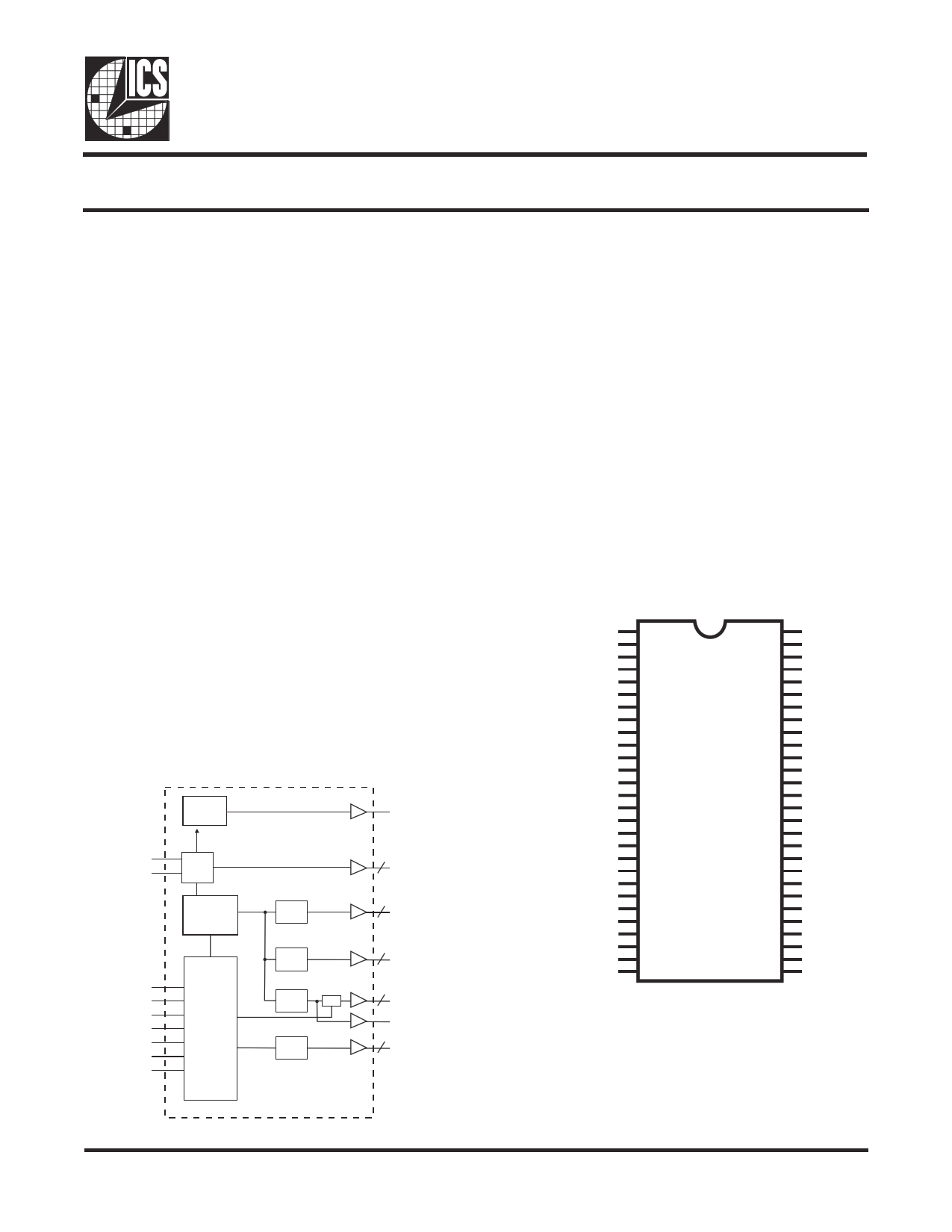
Block Diagram
PLL2
48MHz
X1 XTAL
X2 OSC
PLL1
Spread
Spectrum
PD#
PCI_STOP#
CPU_STOP#
SPREAD#
SEL 133/100#
SEL0
SEL1
Control
Logic
Config.
Reg.
CPU
DIVDER
IOAPIC
DIVDER
PCI
DIVDER
Stop
3V66
DIVDER
REF (1:0)
2
CPUCLK (5:0)
6
IOAPIC (2:0)
3
PCICLK (4:0)
5
PCICLK_F
3V66 (1:0)
2
Features
• Generates the following system clocks:
- 6 CPU clocks ( 2.5V, 100/133MHz)
- 6 PCI clocks, including 1 free running(3.3V,
33MHz)
- 3 IOAPIC clocks (2.5V, 16.67MHz)
- 2 Fixed frequency 66MHz clocks(3.3V, 66MHz)
- 2 REF clocks(3.3V, 14.318MHz)
- 1 USB clock (3.3V, 48MHz)
• Efficient power management through PD#,
CPU_STOP# and PCI_STOP#.
• 0.5% typical down spread modulation on CPU, PCI,
IOAPIC and 3V66 output clocks.
• Uses external 14.318MHz crystal.
Pin Configuration
GND
REF0
REF1
VDD
X1
X2
GND
GND
PCICLK_F
VDD
PCICLK0
PCICLK1
GND
PCICLK2
PCICLK3
VDD
VDD
PCICLK4
GND
GND
GND
VDD
VDD
GND
3V66_0
3V66_1
VDD
SEL 133/100#
1
2
3
4
5
6
7
8
9
10
11
12
13
14
15
16
17
18
19
20
21
22
23
24
25
26
27
28
56 VDDL
55 IOAPIC2
54 IOAPIC1
53 IOAPIC0
52 GND
51 VDDL
50 CPUCLK5
49 CPUCLK4
48 GND
47 VDDL
46 CPUCLK3
45 CPUCLK2
44 GND
43 VDDL
42 CPUCLK1
41 CPUCLK0
40 GND
39 VDD
38 GND
37 PCI_STOP#
36 CPU_STOP#
35 PD#
34 SPREAD#
33 SEL1
32 SEL0
31 VDD
30 48MHz
29 GND
56-pin 300 mil SSOP
56-pin 240 mil TSSOP
0427C—07/03/02
1 page 
ICS932S200
PCI_STOP# Timing Diagram
PCI_STOP# is an input to the clock synthesizer and must be made synchronous to the clock driver PCICLK_F output.
It is used to turn off the PCI clocks for low power operation. PCI clocks are required to be stopped in a low state and
started such that a full high pulse width is guaranteed. ONLY one rising edge of PCICLK_F is allowed after the clock
control logic switched for the PCI outputs to become enabled/disabled.
CPUCLK
(internal)
PCICLK
(internal)
CPU_STOP#
PCI_STOP#
PD#
PCICLK
(externall)
Notes:
1. All timing is referenced to CPUCLK.
2. Internal means inside the chip.
3. All other clocks continue to run undisturbed.
4. PD# and CPU_STOP# are shown in a high state.
5. Diagrams shown with respect to 133MHz. Similar operation when CPU is 100MHz.
0427C—07/03/02
5
5 Page 
ICS932S200
N
INDEX
AREA
12
D
c
E1 E
L
h x 45°
α
A
A1
-C-
e
b
SEATING
PLANE
.10 (.004) C
300 mil SSOP
SYMBOL
In Millimeters
In Inches
COMMON DIMENSIONS COMMON DIMENSIONS
MIN MAX MIN MAX
A
2.413
2.794
.095
.110
A1
0.203
0.406
.008
.016
b
0.203
0.343
.008
.0135
c
0.127
0.254
.005
.010
D
SEE VARIATIONS
SEE VARIATIONS
E
10.033
10.668
.395
.420
E1
7.391
7.595
.291
.299
e 0.635 BASIC 0.025 BASIC
h
0.381
0.635
.015
.025
L
0.508
1.016
.020
.040
N
SEE VARIATIONS
SEE VARIATIONS
α 0° 8° 0° 8°
VARIATIONS
D mm.
N
MIN MAX
56
18.288
18.542
D (inch)
MIN MAX
.720
JEDEC MO-118
DOC# 10-0034
.730
6/1/00
REV B
Ordering Information
ICS932S200yF-T
Example:
ICS XXXX y F - PPP - T
Designation for tape and reel packaging
Pattern Number (2 or 3 digit number for parts with ROM code
patterns)
Package Type
F=SSOP
Revision Designator (will not correlate with datasheet revision)
Device Type (consists of 3 or 4 digit numbers)
Prefix
ICS, AV = Standard Device
0427C—07/03/02
11
11 Page | ||
| Páginas | Total 12 Páginas | |
| PDF Descargar | [ Datasheet ICS932S200.PDF ] | |
Hoja de datos destacado
| Número de pieza | Descripción | Fabricantes |
| ICS932S200 | Frequency Timing Generator | Integrated Circuit Systems |
| ICS932S202 | Frequency Timing Generator | Integrated Circuit Systems |
| ICS932S203 | Frequency Generator | IDT |
| ICS932S203 | Preliminary Product Preview | Integrated Circuit Systems |
| Número de pieza | Descripción | Fabricantes |
| SLA6805M | High Voltage 3 phase Motor Driver IC. |
Sanken |
| SDC1742 | 12- and 14-Bit Hybrid Synchro / Resolver-to-Digital Converters. |
Analog Devices |
|
DataSheet.es es una pagina web que funciona como un repositorio de manuales o hoja de datos de muchos de los productos más populares, |
| DataSheet.es | 2020 | Privacy Policy | Contacto | Buscar |