|
|
|
PDF DG4053E Data sheet ( Hoja de datos )
| Número de pieza | DG4053E | |
| Descripción | Analog Multiplexers | |
| Fabricantes | Vishay | |
| Logotipo | ||
Hay una vista previa y un enlace de descarga de DG4053E (archivo pdf) en la parte inferior de esta página. Total 20 Páginas | ||
|
No Preview Available !
www.vishay.com
DG4051E, DG4052E, DG4053E
Vishay Siliconix
Low Capacitance, Low Charge Injection, 4- / 8-Channel,
Triple SPDT, ± 5 V / 12 V / 5 V / 3 V Analog Multiplexers
DESCRIPTION
The DG4051E, DG4052E, and DG4053E are high precision
CMOS analog multiplexers. The DG4051E is an 8-channel
multiplexer, the DG4052E is a dual 4-channel multiplexer,
and the DG4053E is a triple 2-channel multiplexer or triple
SPDT.
The DG4051E, DG4052E, and DG4053E feature low
leakage, parasitic capacitance, and low charge injection
of 0.3 pC over the full voltage range. These devices are ideal
for high precision signal switching and multiplexing.
Designed to operate from a 3 V to 16 V single supply or from
a ± 3 V to ± 8 V dual supplies, the DG4051E, DG4052E, and
DG4053E are fully specified at 3 V, 5 V, 12 V and ± 5 V. All
control logic inputs have guaranteed 2 V logic high limit
when operating from 5 V or ± 5 V supplies and 1.4 V when
operating from a 3 V supply.
All switches conduct equally well in both directions, offering
rail to rail analog signal switching and can be used both as
multiplexers as well as de-multiplexers.
The DG4051E, DG4052E, and DG4053E operating
temperature is specified from -40 °C to +125 °C and
are available in 16 pin TSSOP and the ultra compact
1.8 mm x 2.6 mm miniQFN16 packages.
BENEFITS
• Wide operation voltage range
• Low charge injection
• Low parasitic capacitance
• Compact package option
FEATURES
• 3 V to 16 V single supply or ± 3 to ± 8 V dual
supply operation
• Low parasitic capacitance:
CD(ON): 8.5 pF / typ. (DG4053E)
CS(OFF): 2.0 pF / typ. (DG4053E)
• Less than 0.3 pC charge injection over the full signal swing
range
• Low leakage: < 50 pA, typ.
• Fast switching tON: 35 ns, typ.
• 3 V logic compatible for control
• Bi-directional rail to rail signal switching
• Material categorization: for definitions of compliance
please see www.vishay.com/doc?99912
APPLICATIONS
• Automatic test equipment
• Process control and automation
• Data acquisition systems
• Meters and instruments
• Medical and healthcare systems
• Communication systems
• Audio and video signal routing
• Relay replacement
• Battery powered systems
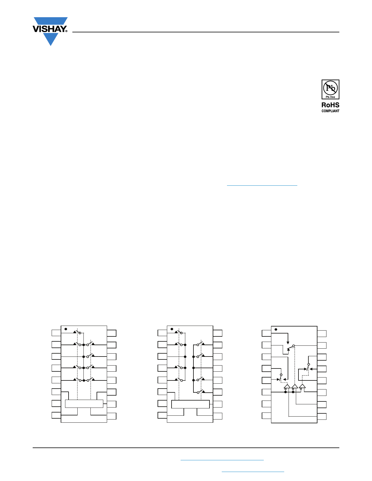
FUNCTIONAL BLOCK DIAGRAM AND PIN CONFIGURATION
DG4051E
TSSOP16
DG4052E
TSSOP16
DG4053E
TSSOP16
X4 1
X6 2
X3
X7 4
X5 5
ENABLE 6
V- 7
GND 8
Logic
16 V+
15 X2
14 X1
13 X0
12 X3
11 A
10 B
9C
Y0 1
Y2 2
Y3
Y3 4
Y1 5
ENABLE 6
V- 7
GND 8
Logic
16 V+
15 X2
14 X1
13 X
12 X0
11 X3
10 A
9B
Y1 1
Y0 2
Z1 3
Z4
Z0 5
EENNAABLE 6
V- 7
GND 8
16 V+
15 Y
14 X
13 X1
12 X0
11 A
10 B
9C
Top View
Top View
ENABLE = LO, all switches are controlled by addr pins.
ENABLE = HI, all switches are off.
Top View
S16-0623-Rev. A, 11-Apr-16
1
Document Number: 69685
For technical questions, contact: [email protected]
THIS DOCUMENT IS SUBJECT TO CHANGE WITHOUT NOTICE. THE PRODUCTS DESCRIBED HEREIN AND THIS DOCUMENT
ARE SUBJECT TO SPECIFIC DISCLAIMERS, SET FORTH AT www.vishay.com/doc?91000
1 page 
www.vishay.com
DG4051E, DG4052E, DG4053E
Vishay Siliconix
SPECIFICATIONS FOR UNIPOLAR SUPPLIES
PARAMETER
Analog Switch
SYMBOL
TEST CONDITIONS
UNLESS OTHERWISE SPECIFIED
V+ = 12 V, V- = 0 V
VIN(A, B, C, and enable) = 2 V, 0.8 V a
Analog Signal Range e VANALOG
On-Resistance
RON IS = 1 mA, VD = 0.7 V, 11.3 V
On-Resistance Match RON
On-Resistance
Flatness
RFLATNESS
IS = 1 mA, VD = 11.3 V
IS = 1 mA, VD = 0.7 V, 11.3 V
Switch Off
Leakage Current
IS(off)
ID(off)
Channel On
Leakage Current
ID(on)
Digital Control
Input Current,
VIN Low
Input Current,
VIN High
Dynamic Characteristics
IL
IH
Transition Time
tTRANS
V+ = 13.2 V, V- = 0 V
VD = 1 V / 12.2 V, VS = 12.2 V / 1 V
V+ = 13.2 V, V- = 0 V
VD = VS = 1 V / 12.2 V
VIN(A, B, C, and enable)
under test = 0.8 V
VIN(A, B, C, and enable)
under test = 2 V
Enable Turn-On Time
Enable Turn-Off Time
Break-Before-Make
Time Delay
Charge Injection e
Off Isolation e
Channel-to-Channel
Crosstalk e
Source Off
Capacitance e
tON
tOFF
tD
Q
OIRR
XTALK
CS(off)
Drain Off
Capacitance e
CD(off)
Channel On
Capacitance e
Power Supplies
Power Supply Current
Negative Supply
Current
Ground Current
CD(on)
I+
I-
IGND
RL = 300 , CL = 35 pF
see Fig. 1, 2, 3
Vg = 0 V, Rg = 0 , CL = 1 nF
RL = 50 , CL = 1 pF
f = 100 kHz
f = 1 MHz
f = 1 MHz
f = 1 MHz
DG4051E
DG4052E
DG4053E
DG4051E
DG4052E
DG4053E
DG4051E
DG4052E
DG4053E
VIN(A, B, C, and enable) = 0 V or 5 V
-40 °C to +125 °C -40 °C to +85 °C
TEMP. b TYP. c
UNIT
MIN. d MAX. d MIN. d MAX. d
Full - 0 12 0 12 V
Room 85 - 103 - 103
Full -
- 133 - 125
Room 1.24
-
8
-8
Full -
-
8
-8
Room 27
-
37
- 37
Full - - 44 - 43
Room ± 0.05 -1 1 -1 1
Full - -50 50 -5 5
Room ± 0.05 -1 1 -1 1
nA
Full - -50 50 -5 5
Room ± 0.05 -1 1 -1 1
Full - -50 50 -5 5
Full 0.02 -1 1 -1 1
μA
Full 0.02 -1 1 -1 1
Room
Full
Room
Full
Room
Full
Room
Full
Full
Room
Room
Room
Room
Room
Room
Room
Room
Room
Room
Room
43
-
22
-
47
-
25
-
-
-
-
-
-
-
-
-
-
-
-
-
-
-
-
-
-
-
1
-
-
-
-
-
-
-
-
-
-
-
-
-
83 - 83
95 - 90
62 - 62
71 - 67
ns
87 - 87
94 - 93
- 1-
- --
- - - pC
- --
dB
- --
- --
- --
- --
- --
- - - pF
- --
- --
- --
- --
Room 0.05
-
1
-1
Full - - 10 - 10
Room -0.05 -1 - -1 -
μA
Full - -10 - -10 -
Room -0.05 -1 - -1 -
Full - -10 - -10 -
S16-0623-Rev. A, 11-Apr-16
5
Document Number: 69685
For technical questions, contact: [email protected]
THIS DOCUMENT IS SUBJECT TO CHANGE WITHOUT NOTICE. THE PRODUCTS DESCRIBED HEREIN AND THIS DOCUMENT
ARE SUBJECT TO SPECIFIC DISCLAIMERS, SET FORTH AT www.vishay.com/doc?91000
5 Page 
www.vishay.com
SCHEMATIC DIAGRAM (Typical Channel)
V+
DG4051E, DG4052E, DG4053E
Vishay Siliconix
A, B
GND
C
EN
V-
V-
V-
V-
Level
shift
Decode/
drive
Body
snatcher
X, Y, Z
V+ V-
X0, Y0, Z0
Xn, Yn, Zn
TEST CIRCUITS
V+
50 Ω
A X0
B
C
X1 - X6
DG4051E
X7
ENABLE
X
VX0
VX7
GND
300 Ω
V-
V+
VO
35 pF
50 Ω
A X0 or Y0
B
X1 - X2 or
Y1 - Y2
DG4052E
X3 or Y3
ENABLE
X or Y
VX0 or VY0
VX3or VY3
VO
GND
300 Ω
35 pF
V-
V+
VA,B,C
V+
0V
50 %
VX0 or VY0 or VZ0
VO
VX7
VX3 or VY3
VX1 or VY1or VZ1
90 %
tTRANS
X0 or Y0 or Z0 ON
X7 ON (DG4051E)
or
X3 or Y3 ON (DG4052E)
or
X1 or Y1 or Z1 ON
(DG4053E)
90 %
tTRANS
50 Ω
A or B
or C
X0 or Y0
or Z0
VX0 or VY0 or VZ0
DG4053E
X1 or Y1 or Z1
ENABLE X or Y or Z
VX1or VY1or VZ1
VO
GND
300 Ω
35 pF
V-
Fig. 1 - Transition Time
S16-0623-Rev. A, 11-Apr-16
11
Document Number: 69685
For technical questions, contact: [email protected]
THIS DOCUMENT IS SUBJECT TO CHANGE WITHOUT NOTICE. THE PRODUCTS DESCRIBED HEREIN AND THIS DOCUMENT
ARE SUBJECT TO SPECIFIC DISCLAIMERS, SET FORTH AT www.vishay.com/doc?91000
11 Page | ||
| Páginas | Total 20 Páginas | |
| PDF Descargar | [ Datasheet DG4053E.PDF ] | |
Hoja de datos destacado
| Número de pieza | Descripción | Fabricantes |
| DG4053A | (DG4051A - DG4053A) Multiplexers | Vishay Siliconix |
| DG4053E | Analog Multiplexers | Vishay |
| Número de pieza | Descripción | Fabricantes |
| SLA6805M | High Voltage 3 phase Motor Driver IC. |
Sanken |
| SDC1742 | 12- and 14-Bit Hybrid Synchro / Resolver-to-Digital Converters. |
Analog Devices |
|
DataSheet.es es una pagina web que funciona como un repositorio de manuales o hoja de datos de muchos de los productos más populares, |
| DataSheet.es | 2020 | Privacy Policy | Contacto | Buscar |