|
|
|
PDF BD6360GUL Data sheet ( Hoja de datos )
| Número de pieza | BD6360GUL | |
| Descripción | Lens Driver | |
| Fabricantes | ROHM Semiconductor | |
| Logotipo | ||
Hay una vista previa y un enlace de descarga de BD6360GUL (archivo pdf) en la parte inferior de esta página. Total 18 Páginas | ||
|
No Preview Available !
Datasheet
Mobile Phone Module Driver
Parallel Interface Type
Lens Driver for Stepping Motor
BD6360GUL
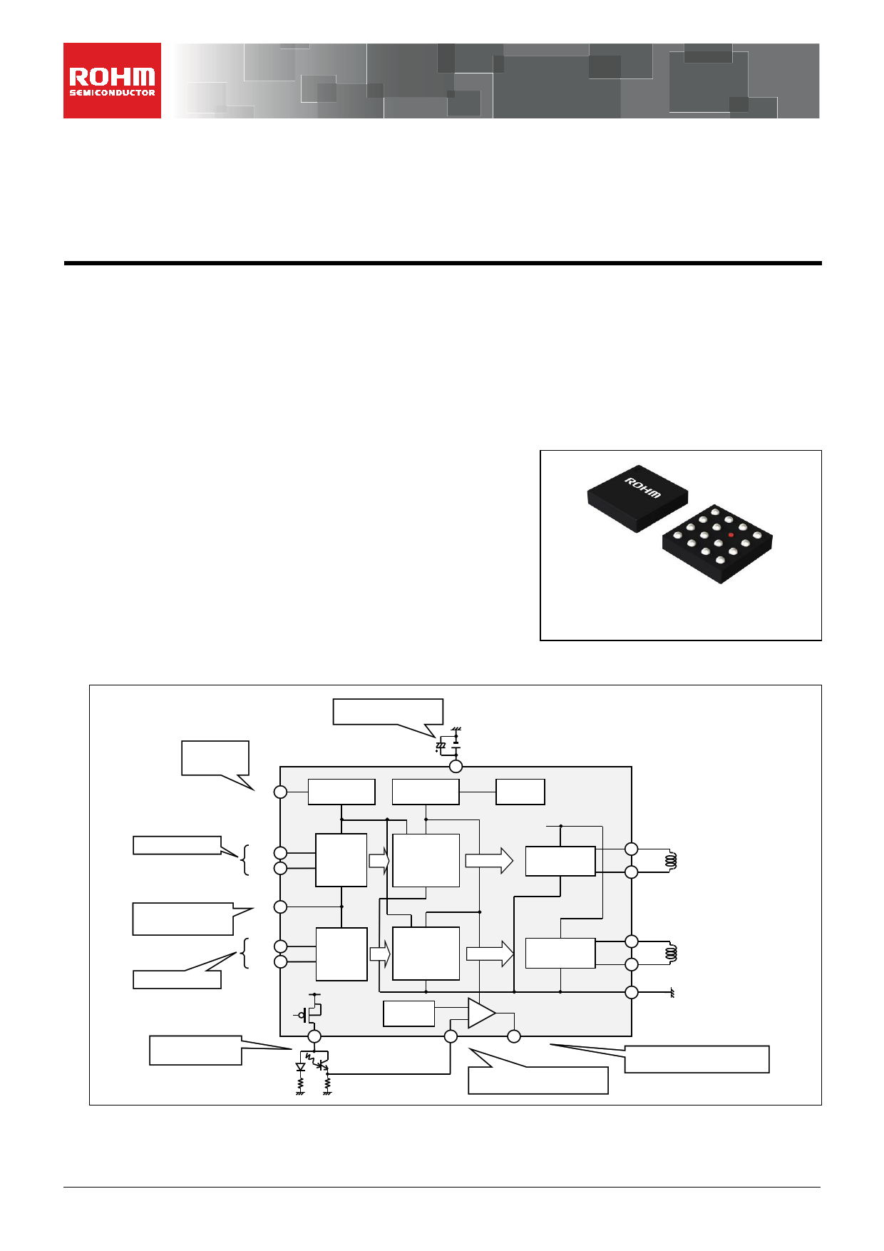
General Description
The BD6360GUL is a motor driver with dual, built-in
Full-ON type two H-Bridges. It also has a power supply
function for photo-interrupter to detect motor position
and wave-shaping circuit built-in. This small surface
mounting package CSP is most suitable for mobile
system and home appliance.
Features
Low ON-Resistance Power CMOS Output
ESD Protection: 8kV, Human Body Model (HBM)
Drive Mode Switch Function
Control Input Pins Fit the Signal of 1.8V System
Voltage-Regulator for Photo-Interrupter and
Comparator with Hysteresis to Convert to Sharp
Waveform
Under Voltage Locked Out protection
& Thermal Shut Down Circuit
Key Specifications
Power Supply Voltage Range:
Circuit Current (No load):
Stand-By Current:
Control Input Voltage Range:
H-Bridge Output Current:
Output ON-Resistance (Total):
Operating Temperature Range:
2.3V to 5.5V
1.1mA(Typ)
5μA (Max)
0V to VCCV
-0.4A to +0.4A
1.0Ω(Typ)
-25°C to +85°C
Package
VCSP50L2
W(Typ) x D(Typ) x H(Max)
2.10mm x 2.10mm x 0.55mm
Applications
Mobile system
Home appliance
Amusement system, etc
VCSP50L2
Typical Application Circuit
Power-saving
H: Active
L: Stand-by
PS 4D
Bypass filter Capacitor for
power supply input
1µF to 100µF
VCC
4B
Power Save
TSD & UVLO
BandGap
Motor control input
IN1A 3D
IN1B 2C
Selectable Drive Mode
H : IN/IN
L : EN/IN
Motor control input
SEL 4C
IN2A 3B
IN2B 3C
Logic
Logic
VCC
Regulator
for
photo-interrupter
4A
BIAS
Level Shift
&
Pre Driver
VCC
H-Bridge
Full ON
OUT1A
1D
1C
OUT1B
Level Shift
&
Pre Driver
H-Bridge
Full ON
VREF
-
+
2A
CIN
3A
COUT
Comparator input for
converting to sharp waveform
OUT2A
1B
1A
OUT2B
GND
2D
Comparator output for
converting to sharp waveform
○Product structure:Silicon monolithic integrated circuit
www.rohm.com
© 2015 ROHM Co., Ltd. All rights reserved.
TSZ22111・14・001
○This product has no designed protection against radioactive rays
1/14
TSZ02201-0H3H0B101420-1-2
09.Dec.2015 Rev.001
1 page 
BD6360GUL
Typical Performance Curves (Reference Data)
5.0
Top 85°C
Mid 25°C
Low -25°C
4.0
Operating range
(2.3V to 5.5V)
3.0
2.0
1.0
0.0
0.0
1.0 2.0 3.0 4.0 5.0 6.0
Power Supply Voltage : VCC [V]
7.0
Figure 1.
Standby Current vs Supply Voltage
3.5
Top 85°C
Mid 25°C
3.0 Low -25°C
2.5 Operating range
(2.3V to 5.5V)
2.0
1.5
1.0
0.5
0.0
0.0
1.0 2.0 3.0 4.0 5.0 6.0
Power Supply Voltage : VCC [V]
7.0
Figure 2.
Circuit Current vs Supply Voltage
0.5
Top 85°C
Mid 25°C
Low -25°C
0.4
Operating range
(0A to 0.4A)
0.3
0.2
0.1
0.0
0.0
0.1 0.2 0.3 0.4
Output Current : IOUT [A]
0.5
Figure 3.
Low Side Output Voltage vs Output Current
0.0
-0.2
-0.4
Operating range
(0A to 0.4A)
-0.6
-0.8
-1.0
0.0
Top -25°C
Mid 25°C
Low 85°C
0.1 0.2 0.3 0.4
Output Current : IOUT [A]
0.5
Figure 4.
High Side Output Voltage vs Output Current
www.rohm.com
© 2015 ROHM Co., Ltd. All rights reserved.
TSZ22111・14・001
5/14
TSZ02201-0H3H0B101420-1-2
09.Dec.2015 Rev.001
5 Page 
BD6360GUL
Operational Notes – continued
12. Regarding the Input Pin of the IC
This monolithic IC contains P+ isolation and P substrate layers between adjacent elements in order to keep them
isolated. P-N junctions are formed at the intersection of the P layers with the N layers of other elements, creating a
parasitic diode or transistor. For example (refer to figure below):
When GND > Pin A and GND > Pin B, the P-N junction operates as a parasitic diode.
When GND > Pin B, the P-N junction operates as a parasitic transistor.
Parasitic diodes inevitably occur in the structure of the IC. The operation of parasitic diodes can result in mutual
interference among circuits, operational faults, or physical damage. Therefore, conditions that cause these diodes to
operate, such as applying a voltage lower than the GND voltage to an input pin (and thus to the P substrate) should be
avoided.
Pin A
P+
NN
Parasitic
Elements
Resistor
Transistor (NPN)
Pin A
Pin B
C
B
E
Pin B
P P+
NN
P Substrate
Parasitic
Elements
N P+
N P N P+ N
P Substrate
B
GND
Parasitic
GND
Elements
Figure 9.
Example of monolithic IC structure
GND
N Region
close-by
C
E
Parasitic
Elements
GND
13. Ceramic Capacitor
When using a ceramic capacitor, determine the dielectric constant considering the change of capacitance with
temperature and the decrease in nominal capacitance due to DC bias and others.
14. Area of Safe Operation (ASO)
Operate the IC such that the output voltage, output current, and power dissipation are all within the Area of Safe
Operation (ASO).
15. Thermal Shutdown Circuit(TSD)
This IC has a built-in thermal shutdown circuit that prevents heat damage to the IC. Normal operation should always
be within the IC’s power dissipation rating. If however the rating is exceeded for a continued period, the junction
temperature (Tj) will rise which will activate the TSD circuit that will turn OFF all output pins. When the Tj falls below
the TSD threshold, the circuits are automatically restored to normal operation.
Note that the TSD circuit operates in a situation that exceeds the absolute maximum ratings and therefore, under no
circumstances, should the TSD circuit be used in a set design or for any purpose other than protecting the IC from
heat damage.
16. Disturbance light
In a device where a portion of silicon is exposed to light such as in a WL-CSP, IC characteristics may be affected due
to photoelectric effect. For this reason, it is recommended to come up with countermeasures that will prevent the chip
from being exposed to light.
www.rohm.com
© 2015 ROHM Co., Ltd. All rights reserved.
TSZ22111・15・001
11/14
TSZ02201-0H3H0B101420-1-2
09.Dec.2015 Rev.001
11 Page | ||
| Páginas | Total 18 Páginas | |
| PDF Descargar | [ Datasheet BD6360GUL.PDF ] | |
Hoja de datos destacado
| Número de pieza | Descripción | Fabricantes |
| BD6360GUL | Lens Driver | ROHM Semiconductor |
| Número de pieza | Descripción | Fabricantes |
| SLA6805M | High Voltage 3 phase Motor Driver IC. |
Sanken |
| SDC1742 | 12- and 14-Bit Hybrid Synchro / Resolver-to-Digital Converters. |
Analog Devices |
|
DataSheet.es es una pagina web que funciona como un repositorio de manuales o hoja de datos de muchos de los productos más populares, |
| DataSheet.es | 2020 | Privacy Policy | Contacto | Buscar |