|
|
|
PDF 9DB1933 Data sheet ( Hoja de datos )
| Número de pieza | 9DB1933 | |
| Descripción | Nineteen Output Differential Buffer | |
| Fabricantes | IDT | |
| Logotipo | ||
Hay una vista previa y un enlace de descarga de 9DB1933 (archivo pdf) en la parte inferior de esta página. Total 17 Páginas | ||
|
No Preview Available !
Nineteen Output Differential Buffer for PCIe Gen3
DATASHEET
9DB1933
Recommended Application
19 output PCIe Gen3 zero-delay/fanout buffer
General Description
The 9DB1933 zero-delay buffer supports PCIe Gen3
requirements, while being backwards compatible to PCIe Gen2
and Gen1. The 9DB1933 is driven by a differential SRC output
pair from an IDT 932S421, 932SQ420, or equivalent, main
clock generator. It attenuates jitter on the input clock and has a
selectable PLL bandwidth to maximize performance in systems
with or without Spread-Spectrum clocking.
Output Features
• 19 - 0.7V current mode differential HCSL output pairs
Features/Benefits
• 8 Selectable SMBus Addresses/Mulitple devices can share
the same SMBus Segment
• 11 dedicated and 3 group OE# pins/Hardware control of the
outputs
• PLL or bypass mode/PLL can dejitter incoming clock
• Selectable PLL bandwidth/minimizes jitter peaking in
downstream PLL's
• Spread Spectrum Compatible/tracks spreading input clock
for low EMI
• SMBus Interface/unused outputs can be disabled
• Supports undriven differential outputs in Power Down mode
for power management
Key Specifications
• Cycle-to-cycle jitter <50ps
• Output-to-output skew < 150 ps
• PCIe Gen3 phase jitter < 1.0ps RMS
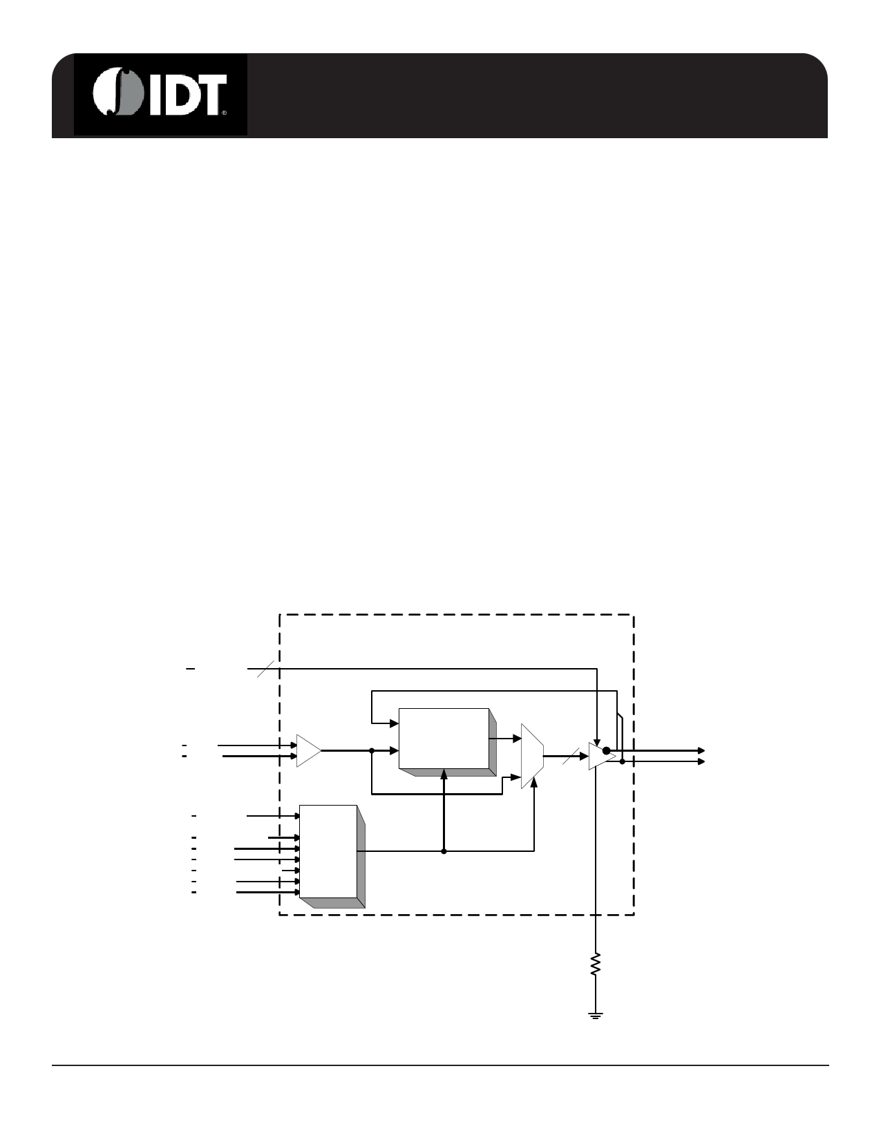
Functional Block Diagram
OE(17_18)#
OE(15_16)#
OE(14:5)#,
OE_01234#
13
DIF_IN
DIF_IN#
HIGH_BW#
CKPWRGD/PD#
SMB_A0
SMB_A1
SMB_A2_PLLBYP#
SMBDAT
SMBCLK
Logic
PLL
(SS Compatible)
19
DIF(18:0)
IREF
IDT® Nineteen Output Differential Buffer for PCIe Gen3
1
1676A—07/12/10
1 page 
9DB1933
Nineteen Output Differential Buffer for PCIe Gen3
Electrical Characteristics - Absolute Maximum Ratings
PARAMETER
SYMBOL
CONDITIONS
3.3V Core Supply Voltage VDDA
3.3V Logic Supply Voltage VDD
Input Low Voltage
VIL
Input High Voltage
VIH
Except for SMBus interface
Input High Voltage
VIHSMB
SMBus clock and data pins
Storage Temperature
Ts
Junction Temperature
Tj
Input ESD protection ESD prot
Human Body Model
1Guaranteed by design and characterization, not 100% tested in production.
2 Operation under these conditions is neither implied nor guaranteed.
MIN
GND-0.5
-65
2000
TYP
MAX UNITS NOTES
4.6 V 1,2
4.6 V 1,2
V1
VDD+0.5V
5.5V
V
V
1
1
150 °C 1
125 °C 1
V1
Electrical Characteristics - Input/Supply/Common Parameters
TA = TCOM; Supply Voltage VDD = 3.3 V +/-5%
PARAMETER
SYMBOL
CONDITIONS
Ambient Operating
Temperature
Input High Voltage
TCOM
VIH
Commmercial range
Single-ended inputs, except SMBus, low
threshold and tri-level inputs
Input Low Voltage
VIL
Single-ended inputs, except SMBus, low
threshold and tri-level inputs
IIN Single-ended inputs, VIN = GND, VIN = VDD
MIN TYP
0
2
GND - 0.3
-5
MAX UNITS NOTES
70
VDD + 0.3
°C
V
1
1
0.8 V 1
5 uA 1
Input Current
Single-ended inputs
IINP
VIN = 0 V; Inputs with internal pull-up resistors
-200
VIN = VDD; Inputs with internal pull-down resistors
200 uA 1
Input Frequency
Pin Inductance
Capacitance
Clk Stabilization
Fibyp
Fipll
Lpin
CIN
CINDIF_IN
VDD = 3.3 V, Bypass mode
VDD = 3.3 V, 100MHz PLL mode
Logic Inputs, except DIF_IN
DIF_IN differential clock inputs
10 166 MHz 2
90 100 110 MHz 2
7 nH 1
1.5 5 pF 1
1.5 2.7 pF 1,4
COUT
Output pin capacitance
2.5 6 pF 1
TSTAB
From VDD Power-Up and after input clock
stabilization or de-assertion of PD# to 1st clock
1.000
1.8
ms 1,2
Input SS Modulation
Frequency
fMODIN
Allowable Frequency
(Triangular Modulation)
30
33 kHz 1
OE# Latency
tLATOE#
DIF start after OE# assertion
DIF stop after OE# deassertion
Tdrive_PD#
tDRVPD
DIF output enable after
PD# de-assertion
Tfall tF Fall time of control inputs
Trise tR Rise time of control inputs
SMBus Input Low Voltage VILSMB
SMBus Input High Voltage VIHSMB
SMBus Output Low Voltage VOLSMB
@ IPULLUP
SMBus Sink Current
IPULLUP
@ VOL
Nominal Bus Voltage
VDDSMB
3V to 5V +/- 10%
SCLK/SDATA Rise Time
tRSMB
(Max VIL - 0.15) to (Min VIH + 0.15)
SCLK/SDATA Fall Time
SMBus Operating
Frequency
tFSMB
fMAXSMB
(Min VIH + 0.15) to (Max VIL - 0.15)
Maximum SMBus operating frequency
1Guaranteed by design and characterization, not 100% tested in production.
2Control input must be monotonic from 20% to 80% of input swing.
3Time from deassertion until outputs are >200 mV
4DIF_IN input
5The differential input clock must be running for the SMBus to be active
IDT® Nineteen Output Differential Buffer for PCIe Gen3
4
2.1
4
2.7
12 cycles 1,3
300
5
5
0.8
VDDSMB
0.4
5.5
1000
300
100
us
ns
ns
V
V
V
mA
V
ns
ns
kHz
1,3
1,2
1,2
1
1
1
1
1
1
1
1,5
1676A—07/12/10
5
5 Page 
9DB1933
Nineteen Output Differential Buffer for PCIe Gen3
Alternative Termination for LVDS and other Common Differential Signals (figure 3)
Vdiff
Vp-p
Vcm
R1
R2
R3
R4
Note
0.45v 0.22v 1.08
33
150 100 100
0.58 0.28 0.6
33
78.7 137
100
0.80 0.40 0.6
33
78.7
none
100
ICS874003i-02 input compatible
0.60 0.3 1.2 33
174 140 100 Standard LVDS
R1a = R1b = R1
R2a = R2b = R2
Figure 3
L1 L2
R1a
R3
L4
L4'
L1' L2'
HCSL Output Buffer
R1b
R2a
R2b
L3' L3
R4
Down Device
REF_CLK Input
Cable Connected AC Coupled Application (figure 4)
Component
Value
Note
R5a, R5b
8.2K 5%
R6a, R6b
1K 5%
Cc 0.1 µF
Vcm
0.350 volts
Figure 4
3.3 Volts
Cc
Cc
R5a R5b
L4
L4'
R6a R6b
PCIe Device
REF_CLK Input
IDT® Nineteen Output Differential Buffer for PCIe Gen3
11
1676A—07/12/10
11 Page | ||
| Páginas | Total 17 Páginas | |
| PDF Descargar | [ Datasheet 9DB1933.PDF ] | |
Hoja de datos destacado
| Número de pieza | Descripción | Fabricantes |
| 9DB1933 | Nineteen Output Differential Buffer | IDT |
| Número de pieza | Descripción | Fabricantes |
| SLA6805M | High Voltage 3 phase Motor Driver IC. |
Sanken |
| SDC1742 | 12- and 14-Bit Hybrid Synchro / Resolver-to-Digital Converters. |
Analog Devices |
|
DataSheet.es es una pagina web que funciona como un repositorio de manuales o hoja de datos de muchos de los productos más populares, |
| DataSheet.es | 2020 | Privacy Policy | Contacto | Buscar |