|
|
|
PDF BD63536FJ Data sheet ( Hoja de datos )
| Número de pieza | BD63536FJ | |
| Descripción | 3.0V to 30V Input 1ch Buck Controller | |
| Fabricantes | ROHM Semiconductor | |
| Logotipo | ||
Hay una vista previa y un enlace de descarga de BD63536FJ (archivo pdf) en la parte inferior de esta página. Total 21 Páginas | ||
|
No Preview Available !
Datasheet
3.0V to 30V Input 1ch
Buck Controller
BD63536FJ
General Description
The BD63536FJ is a gate direct drive switching
regulator operating at a power supply voltage from 3V
to 30V. This regulator uses a compact package SOP-J8
and operates as a switching regulator for the voltage
control type of step-down DC/DC converter. The
regulator features reliable design with 1% reference
voltage accuracy, built-in current limit function (4%),
and a variety of built-in protection circuits.
Features
Gate Direct Drive Available (External Pch FET,
VCC-5.4V)
Built-in Current Limit Function (150mV4%)
Built-in Gate-off Function
Built-in Soft Start
2.5V Regulator Output Voltage
Variable External Oscillation Frequency
Built-in Thermal Shutdown Circuit
Applications
Laser Beam Printers, MFPs, PPCs, etc.
Key Specifications
Power Supply Voltage Range:
Error Amplifier Reference Voltage:
Output Current (Peak):
Oscillation Frequency:
Operating Temperature Range:
3.0V to 30V
1.25V1%
200mA(Max)
300kHz(Max)
-25°C to +85°C
Package
W(Typ) x D(Typ) x H(Max)
SOP-J8
4.90mm x 6.00mm x 1.65mm
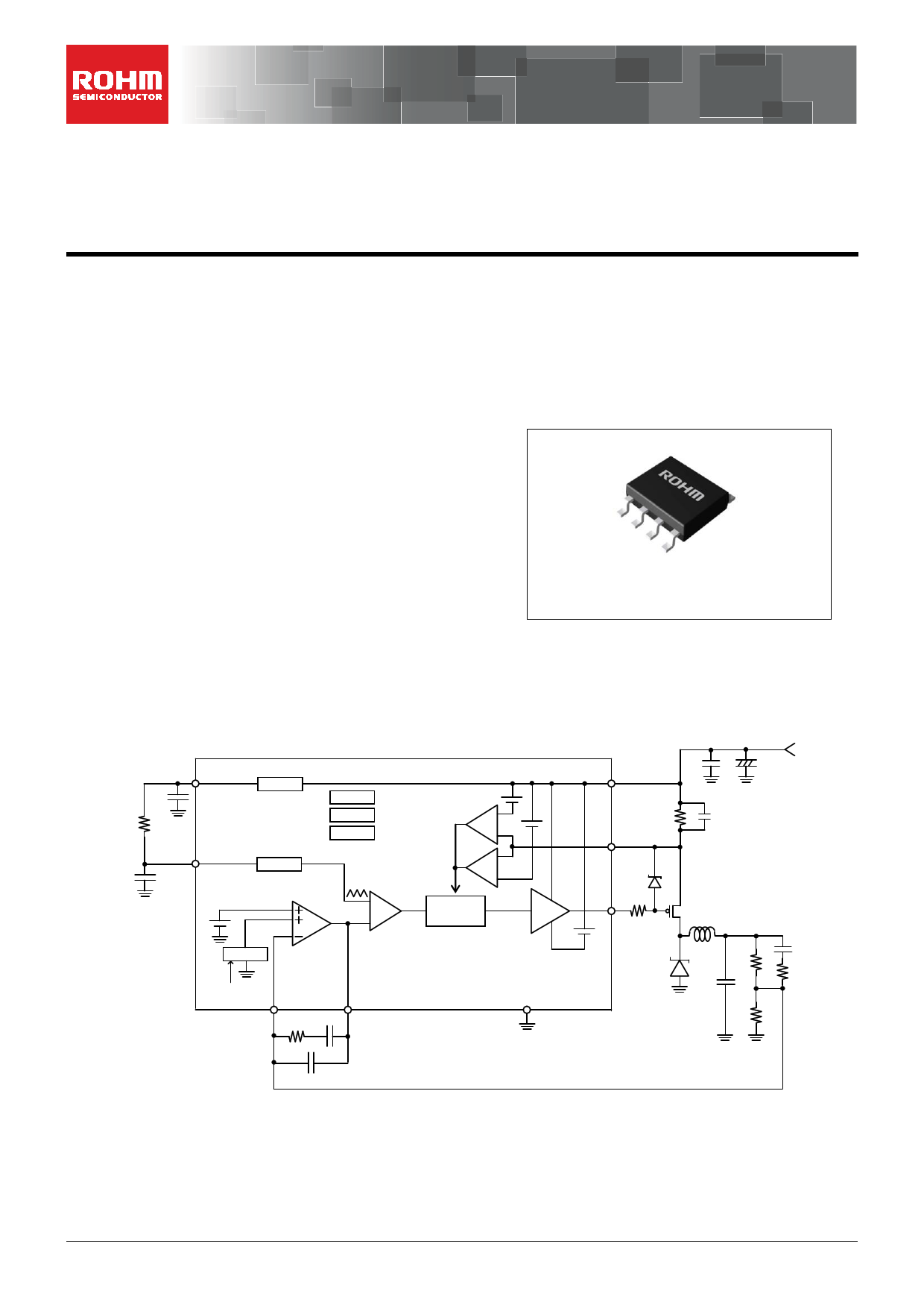
Typical Application Circuit
VREF
VREG
R
OSC
C
OSC
1.25v
Soft Start
GATEOFF、OVP
TSD、UVLO
IN-
UVLO
TSD
OVP
COMP
C.L.
COMP
GATE
OFF
Controller
FB
GND
VCC
CS
GATE
VIN
RFB1
RFB2
Figure 1. Typical Application Circuit
○Product structure:Silicon monolithic integrated circuit
.www.rohm.com
© 2014 ROHM Co., Ltd. All rights reserved.
TSZ22111・14・001
○This product has no designed protection against radioactive rays
1/17
TSZ02201-0P2P0AJ00850-1-2
23.Oct.2014 Rev.001
1 page 
BD63536FJ
Typical Performance Curves - continued
(Unless otherwise specified, Ta25C, VCC 24V)
35
30
25
20
15
10
5
0
3 6 9 12 15 18 21 24 27 30
Power SVuCpCply: V[Vo]ltage : VCC [V]
Figure 6. Gate H Voltage vs Power Supply Voltage
(Output Block)
35
30
25
20
15
10
5
0
3 6 9 12 15 18 21 24 27 30
Power SVuCppCly: V[Vo]ltage : VCC [V]
Figure 7. Gate L Voltage vs Power Supply Voltage
(Output Block)
1.5
1.2
0.9
0.6
0.3
0
0 4 8 12 16 20 24 28 32
Power SuVpCpCly :Vo[Vlt]age : VCC [V]
Figure 8. Reference Voltage vs Power Supply Voltage
(Error Amplifier Block)
1.5
1.2
0.9
0.6
0.3
0
-25 0 25 50 75
TTeemmpepreartautruere: T: aTa[℃[°C]]
Figure 9. Reference Voltage vs Temperature
(Error Amplifier Block)
www.rohm.com
© 2014 ROHM Co., Ltd. All rights reserved.
TSZ22111・15・001
5/17
TSZ02201-0P2P0AJ00850-1-2
23.Oct.2014 Rev.001
5 Page 
BD63536FJ
4. Typical Filter Circuit
When considering a filter circuit for the determination of the phase characteristics with the application of this IC, the three
configurations shown in Figure 19 below are the popular configurations of the filter circuits. The selection of the
configuration to be used is determined by the relationship between the PWM frequency to be used and the second pole
of LC filter, the zero point at ESR of output capacitor, and the ripple elimination rate at the PWM switching frequency to
be used.
VIN
RFB1
RFB2
R2 C0
VOUT
VIN
RFB1
RFB2
C1
R2 C0
VOUT
VOUT
RFB1
C1
R1 C0 R2
RFB2
CF
(a) Filter Example 1
(b) Filter Example 2
(c) Filter Example 3
Figure 19. Examples of Filter Circuits Used to Determine Phase Characteristics
The circuit (a) is the simplest configuration and can be used if the output capacitor has high ESR.
The circuit (b) is a configuration designed by adding a capacitor to the configuration of (a) and can be used if the output
capacitor has high ESR and the voltage ripple elimination rate at the PMW frequency needs to be increased from that of
the configuration of (a).
The circuit (c) is a configuration designed by adding two zero-points and can be used even if the output capacitor has
small ESR.
Select the circuit configuration according to the required specifications and situations for inductors, capacitors, and PWM
frequency.
5. Typical Application Design
The following section shows a typical application design.
VREF
VREG
R
OSC
C
OSC
1.25V
Soft Start
GATEOFF, OVP
TSD, UVLO
IN-
UVLO
TSD
OVP
COMP
C.L.
COMP
GATE
OFF
Controller
FB
GND
VCC
CS
GATE
VIN
RRfFbB11
RRfFbB22
Figure 20. Typical Application Design
www.rohm.com
© 2014 ROHM Co., Ltd. All rights reserved.
TSZ22111・15・001
11/17
TSZ02201-0P2P0AJ00850-1-2
23.Oct.2014 Rev.001
11 Page | ||
| Páginas | Total 21 Páginas | |
| PDF Descargar | [ Datasheet BD63536FJ.PDF ] | |
Hoja de datos destacado
| Número de pieza | Descripción | Fabricantes |
| BD63536FJ | 3.0V to 30V Input 1ch Buck Controller | ROHM Semiconductor |
| Número de pieza | Descripción | Fabricantes |
| SLA6805M | High Voltage 3 phase Motor Driver IC. |
Sanken |
| SDC1742 | 12- and 14-Bit Hybrid Synchro / Resolver-to-Digital Converters. |
Analog Devices |
|
DataSheet.es es una pagina web que funciona como un repositorio de manuales o hoja de datos de muchos de los productos más populares, |
| DataSheet.es | 2020 | Privacy Policy | Contacto | Buscar |