|
|
|
PDF AD7812 Data sheet ( Hoja de datos )
| Número de pieza | AD7812 | |
| Descripción | 10-Bit 4-/8-Channel Sampling ADCs | |
| Fabricantes | Analog Devices | |
| Logotipo | ||
Hay una vista previa y un enlace de descarga de AD7812 (archivo pdf) en la parte inferior de esta página. Total 24 Páginas | ||
|
No Preview Available !
a
2.7 V to 5.5 V, 350 kSPS, 10-Bit
4-/8-Channel Sampling ADCs
AD7811/AD7812
FEATURES
10-Bit ADC with 2.3 s Conversion Time
The AD7811 has Four Single-Ended Inputs that
Can Be Configured as Three Pseudo Differential
Inputs with Respect to a Common, or as Two Inde-
pendent Pseudo Differential Channels
The AD7812 has Eight Single-Ended Inputs that Can
Be Configured as Seven Pseudo Differential Inputs
with Respect to a Common, or as Four Independent
Pseudo Differential Channels
Onboard Track and Hold
Onboard Reference 2.5 V ؎ 2.5%
Operating Supply Range: 2.7 V to 5.5 V
Specifications at 2.7 V–3.6 V and 5 V ؎ 10%
DSP-/Microcontroller-Compatible Serial Interface
High Speed Sampling and Automatic Power-Down Modes
Package Address Pin on the AD7811 and AD7812 Allows
Sharing of the Serial Bus in Multipackage Applications
Input Signal Range: 0 V to VREF
Reference Input Range: 1.2 V to VDD
Qualified for Automotive Applications
GENERAL DESCRIPTION
The AD7811 and AD7812 are high speed, low power, 10-bit
A/D converters that operate from a single 2.7 V to 5.5 V supply.
The devices contain a 2.3 µs successive approximation A/D
converter, an on-chip track/hold amplifier, a 2.5 V on-chip refer-
ence and a high speed serial interface that is compatible with the
serial interfaces of most DSPs (Digital Signal Processors) and
microcontrollers. The user also has the option of using an exter-
nal reference by connecting it to the VREF pin and setting the
EXTREF bit in the control register. The VREF pin may be tied
to VDD. At slower throughput rates the power-down mode may
be used to automatically power down between conversions.
The control registers of the AD7811 and AD7812 allow the
input channels to be configured as single-ended or pseudo
differential. The control register also features a software convert
start and a software power-down. Two of these devices can
share the same serial bus and may be individually addressed in
a multipackage application by hardwiring the device address pin.
The AD7811 is available in a small, 16-lead 0.3" wide, plastic
dual-in-line package (mini-DIP), in a 16-lead 0.15" wide, Small
Outline IC (SOIC) and in a 16-lead, Thin Shrink Small Out-
line Package (TSSOP). The AD7812 is available in a small,
20-lead 0.3" wide, plastic dual-in-line package (mini-DIP), in a
20-lead, Small Outline IC (SOIC) and in a 20-lead, Thin Shrink
Small Outline Package (TSSOP).
PRODUCT HIGHLIGHTS
1. Low Power, Single Supply Operation
Both the AD7811 and AD7812 operate from a single 2.7 V
to 5.5 V supply and typically consume only 10 mW of power.
The power dissipation can be significantly reduced at
lower throughput rates by using the automatic power-
down mode e.g., 315 µW @ 10 kSPS, VDD = 3 V—see
Power vs. Throughput.
2. 4-/8-Channel, 10-Bit ADC
The AD7811 and AD7812 have four and eight single-ended
input channels respectively. These inputs can be configured
as pseudo differential inputs by using the Control Register.
3. On-chip 2.5 V (± 2.5%) reference circuit that is powered
down when using an external reference.
4. Hardware and Software Control
The AD7811 and AD7812 provide for both hardware and
software control of Convert Start and Power-Down.
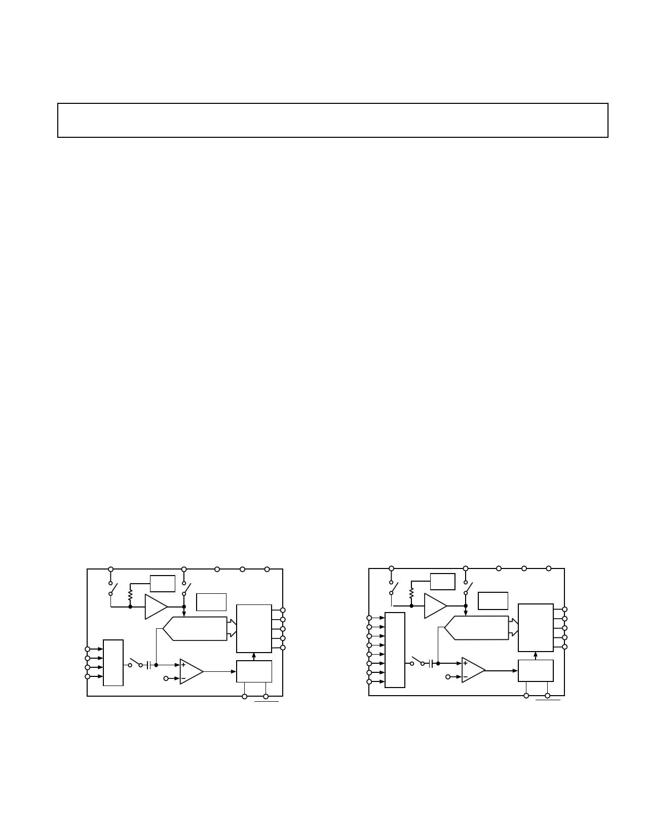
FUNCTIONAL BLOCK DIAGRAMS
CREF
VIN1
VIN2
VIN3
VIN4
MUX
REFIN
VDD AGND DGND
1.23V
REF
BUF
CLOCK
OSC
CHARGE
REDISTRIBUTION
DAC
AD7811
SERIAL
PORT
DOUT
DIN
RFS
TFS
SCLK
VDD /3
COMP
CONTROL
LOGIC
CREF
VIN1
VIN2
VIN3
VIN4
VIN5
VIN6
VIN7
VIN8
MUX
REFIN
VDD AGND DGND
1.23V
REF
BUF
CLOCK
OSC
CHARGE
REDISTRIBUTION
DAC
AD7812
SERIAL
PORT
DOUT
DIN
RFS
TFS
SCLK
VDD /3
COMP
CONTROL
LOGIC
A0 CONVST
A0 CONVST
REV. C
Information furnished by Analog Devices is believed to be accurate and
reliable. However, no responsibility is assumed by Analog Devices for its
use, nor for any infringements of patents or other rights of third parties
which may result from its use. No license is granted by implication or
otherwise under any patent or patent rights of Analog Devices.
One Technology Way, P.O. Box 9106, Norwood, MA 02062-9106, U.S.A.
Tel: 781/329-4700 World Wide Web Site: http://www.analog.com
Fax: 781/326-8703
© Analog Devices, Inc., 2014
1 page 
PIN CONFIGURATIONS
DIP/SOIC/TSSOP
AD7811/AD7812
VREF 1
16 VDD
CREF 2
15 CONVST
VIN1 3
14 SCLK
AD7811
AGND 4
13 DIN
TOP VIEW
VIN2 5 (Not to Scale) 12 DOUT
VIN3 6
11 RFS
VIN4 7
10 TFS
A0 8
9 DGND
VREF 1
CREF 2
20 VDD
19 CONVST
VIN1 3
18 SCLK
AGND 4
17 DIN
VIN2 5 AD7812 16 DOUT
VIN3
6
TOP VIEW
(Not to Scale)
15 RFS
VIN4 7
14 TFS
VIN5 8
VIN6 9
13 DGND
12 A0
VIN7 10
11 VIN8
Pin(s)
AD7811
1
Pin(s)
AD7812
1
Mnemonic
VREF
2
3, 5–7
4
8
2
3, 5–11
4
12
CREF
VIN1–VIN4(8)
AGND
A0
9 13
10 14
11 15
DGND
TFS
RFS
12 16
13 17
14 18
15 19
16 20
REV.CB
DOUT
DIN
SCLK
CONVST
VDD
PIN FUNCTION DESCRIPTIONS
Description
An external reference input can be applied here. When using an external precision
reference or VDD the EXTREF bit in the control register must be set to logic one. The
external reference input range is 1.2 V to VDD.
Reference Capacitor. A capacitor (10 nF) is connected here to improve the noise
performance of the on-chip reference.
Analog Inputs. The analog input range is 0 V to VREF.
Analog Ground. Ground reference for track/hold, comparator, on-chip reference and
DAC.
Package Address Pin. This Logic Input can be hardwired high or low. When used in
conjunction with the package address bit in the control register this input allows two
devices to share the same serial bus. For example a twelve channel solution can be
achieved by using the AD7811 and the AD7812 on the same serial bus.
Digital Ground. Ground reference for digital circuitry.
Transmit Frame Sync. The falling edge of this Logic Input tells the part that a new
control byte should be shifted in on the next 10 falling edges of SCLK.
Receive Frame Sync. The rising edge of this Logic Input is used to enable a counter in
the serial interface. It is used to provide compatibility with DSPs which use a continuous
serial clock and framing signal. In multipackage applications the RFS Pin can also be
used as a serial bus select pin. The serial interface will ignore the SCLK until it receives a
rising edge on this input. The counter is reset at the end of a serial read operation.
Serial Data Output. Serial data is shifted out on this pin on the rising edge of the serial
clock. The output enters a High impedance condition on the rising edge of the 11th
SCLK pulse.
Serial Data Input. The control byte is read in at this input. In order to complete a
serial write operation 13 SCLK pulses need to be provided. Only the first 10 bits are
shifted in—see Serial Interface section.
Serial Clock Input. An external serial clock is applied to this input to obtain serial data
from the AD7811/AD7812 and also to latch data into the AD7811/AD7812. Data is
clocked out on the rising edge of SCLK and latched in on the falling edge of SCLK.
Convert Start. This is an edge triggered logic input. The Track/Hold goes into its Hold
Mode on the falling edge of this signal and a conversion is initiated. The state of this
pin at the end of conversion also determines whether the part is powered down or not.
See operating modes section of this data sheet.
Positive Supply Voltage 2.7 V to 5.5 V.
–5–
5 Page 
AD7811/AD7812
An example of the pseudo differential scheme using the AD7811
is shown in Figure 6. The relevant bits in the AD7811 Control
Register are set as follows DIF/SGL = 1, CH1 = CH2 = 0, i.e.,
VIN1 pseudo differential with respect to VIN2. The signal is
applied to VIN1 but in the pseudo differential scheme the sam-
pling capacitor is connected to VIN2 during conversion and not
AGND as described in the Converter Operation section. This
input scheme can be used to remove offsets that exist in a sys-
tem. For example, if a system had an offset of 0.5 V the offset
could be applied to VIN2 and the signal applied to VIN1. This has
the effect of offsetting the input span by 0.5 V. It is only pos-
sible to offset the input span when the reference voltage is less
than VDD–OFFSET.
VIN1
VOFFSET
VOFFSET
VIN1
VIN2
VIN+
VIN–
SAMPLING
CAPACITOR
CONVERSION
PHASE
VDD/3
CHARGE
REDISTRIBUTION
DAC
CONTROL
LOGIC
COMPARATOR
CLOCK
OSC
Figure 6. Pseudo Differential Input Scheme
When using the pseudo differential input scheme the signal on
VIN2 must not vary by more than a 1/2 LSB during the conver-
sion process. If the signal on VIN2 varies during conversion, the
conversion result will be incorrect. In single-ended mode the
sampling capacitor is always connected to AGND during con-
version. Figure 7 shows the AD7811/AD7812 pseudo differen-
tial input being used to make a unipolar dc current measurement.
A sense resistor is used to convert the current to a voltage and
the voltage is applied to the differential input as shown.
VDD
RSENSE
RL
VIN+
AD7811/
AD7812
VIN–
Figure 7. DC Current Measurement Scheme
DC Acquisition Time
The ADC starts a new acquisition phase at the end of a conver-
sion and ends on the falling edge of the CONVST signal. At the
end of a conversion a settling time is associated with the sam-
pling circuit. This settling time lasts approximately 100 ns. The
analog signal on VIN+ is also being acquired during this settling
time. Therefore, the minimum acquisition time needed is
approximately 100 ns.
Figure 8 shows the equivalent charging circuit for the sampling
capacitor when the ADC is in its acquisition phase. R2 repre-
sents the source impedance of a buffer amplifier or resistive
network; R1 is an internal multiplexer resistance, and C1 is the
sampling capacitor. During the acquisition phase the sampling
capacitor must be charged to within a 1/2 LSB of its final value.
The time it takes to charge the sampling capacitor (TCHARGE) is
given by the following formula:
TCHARGE = 7.6 × (R2 + 125 Ω) × 3.5 pF
R2 VIN+
R1
125⍀
C1
3.5pF
SAMPLING
CAPACITOR
Figure 8. Equivalent Sampling Circuit
For small values of source impedance, the settling time associ-
ated with the sampling circuit (100 ns) is, in effect, the acquisi-
tion time of the ADC. For example, with a source impedance
(R2) of 10 Ω the charge time for the sampling capacitor is
approximately 4 ns. The charge time becomes significant for
source impedances of 2 kΩ and greater.
AC Acquisition Time
In ac applications it is recommended to always buffer analog
input signals. The source impedance of the drive circuitry must
be kept as low as possible to minimize the acquisition time of
the ADC. Large values of source impedance will cause the THD
to degrade at high throughput rates. In addition, better perfor-
mance can generally be achieved by using an External 1 nF
capacitor on VIN.
ON-CHIP REFERENCE
The AD7811 and AD7812 have an on-chip 2.5 V reference
circuit. The schematic in Figure 9 shows how the reference
circuit is implemented. A 1.23 V bandgap reference is gained up
to provide a 2.5 V ± 2% reference voltage. The on-chip refer-
ence is not available externally (SW2 is open). An external refer-
ence (1.2 V to VDD) can be applied at the VREF pin. However in
order to use an external reference the EXTREF bit in the con-
trol register (Bit 0) must first be set to a Logic 1. When EXTREF
is set to a Logic 1 SW2 will close, SW3 will open and the ampli-
fier will power down. This will reduce the current consumption
of the part by about 1 mA. It is possible to use two different
reference voltages by selecting the on-chip reference or external
reference.
EXTERNAL
CAPACITOR
CREF
SW1
1.23V
VREF
SW2
2.5V
7pF
REV.CB
–11–
SW3
AGND
Figure 9. On-Chip Reference Circuitry
11 Page | ||
| Páginas | Total 24 Páginas | |
| PDF Descargar | [ Datasheet AD7812.PDF ] | |
Hoja de datos destacado
| Número de pieza | Descripción | Fabricantes |
| AD781 | Complete 700 ns Sample-and-Hold Amplifier | Analog Devices |
| AD7810 | 10-Bit ADC | Analog Devices |
| AD7811 | 10-Bit 4-/8-Channel Sampling ADCs | Analog Devices |
| AD7812 | 10-Bit 4-/8-Channel Sampling ADCs | Analog Devices |
| Número de pieza | Descripción | Fabricantes |
| SLA6805M | High Voltage 3 phase Motor Driver IC. |
Sanken |
| SDC1742 | 12- and 14-Bit Hybrid Synchro / Resolver-to-Digital Converters. |
Analog Devices |
|
DataSheet.es es una pagina web que funciona como un repositorio de manuales o hoja de datos de muchos de los productos más populares, |
| DataSheet.es | 2020 | Privacy Policy | Contacto | Buscar |