|
|
|
PDF NBC12439 Data sheet ( Hoja de datos )
| Número de pieza | NBC12439 | |
| Descripción | Programmable PLL Synthesized Clock Generator | |
| Fabricantes | ON Semiconductor | |
| Logotipo | ||
Hay una vista previa y un enlace de descarga de NBC12439 (archivo pdf) en la parte inferior de esta página. Total 20 Páginas | ||
|
No Preview Available !
NBC12439, NBC12439A
3.3V/5V Programmable PLL
Synthesized Clock
Generator
50 MHz to 800 MHz
Description
The NBC12439 and NBC12439A are general purpose, PLL based
synthesized clock sources. The VCO will operate over a frequency
range of 400 MHz to 800 MHz. The VCO frequency is sent to the
N--output divider, where it can be configured to provide division ratios
of 1, 2, 4 or 8. The VCO and output frequency can be programmed
using the parallel or serial interfaces to the configuration logic. Output
frequency steps of 16 MHz, 8 MHz, 4 MHz, or 2 MHz can be
achieved using a 16 MHz crystal, depending on the output divider
settings. The PLL loop filter is fully integrated and does not require
any external components.
Features
• Best--in--Class Output Jitter Performance, ±20 ps Peak--to--Peak
• 50 MHz to 800 MHz Programmable Differential PECL Outputs
• Fully Integrated Phase--Lock--Loop with Internal Loop Filter
www.DataSheet4U.com
• Parallel Interface for Programming Counter and Output Dividers
During Powerup
• Minimal Frequency Overshoot
• Serial 3--Wire Programming Interface
• Crystal Oscillator Inputs 10 MHz to 20 MHz
• Operating Range: VCC = 3.135 V to 5.25 V
• CMOS and TTL Compatible Control Inputs
• Pin and Function Compatible with Motorola MC12439 and
MPC9239
• Powerdown of PECL Outputs (÷16)
• 0°C to 70°C Ambient Operating Temperature (NBC12439)
• --40°C to 85°C Ambient Operating Temperature (NBC12439A)
• Pb--Free Packages are Available
http://onsemi.com
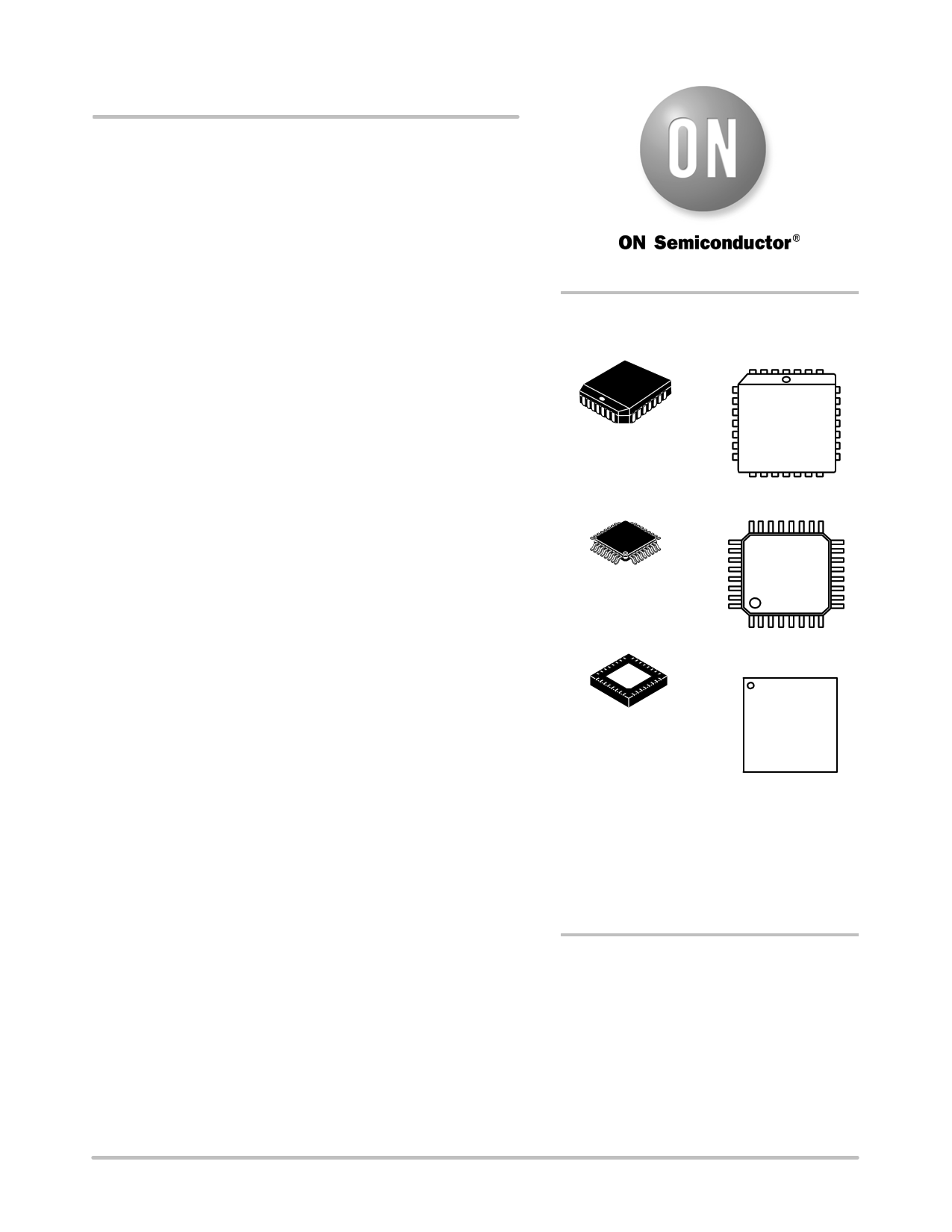
MARKING
DIAGRAMS
1 28
PLCC--28
FN SUFFIX
CASE 776
NBC12439xG
AWLYYWW
LQFP--32
FA SUFFIX
CASE 873A
NBC12
439x
AWLYYWWG
1 32
QFN32
MN SUFFIX
CASE 488AM
1
NBC12
439x
AWLYYWWG
G
x = Blank or A
A = Assembly Location
WL, L = Wafer Lot
YY, Y = Year
WW, W = Work Week
G or G = Pb--Free Package
(Note: Microdot may be in either location)
ORDERING INFORMATION
See detailed ordering and shipping information in the package
dimensions section on page 16 of this data sheet.
© Semiconductor Components Industries, LLC, 2007
February, 2007 -- Rev. 10
1
Publication Order Number:
NBC12439/D
1 page 
NBC12439, NBC12439A
Table 4. ATTRIBUTES
Characteristics
Internal Input Pulldown Resistor
Internal Input Pullup Resistor
ESD Protection
Human Body Model
Machine Model
Charged Device Model
Moisture Sensitivity (Note 1)
PLCC
LQFP
QFN
Flammability Rating
Oxygen Index: 28 to 34
Transistor Count
Meets or exceeds JEDEC Spec EIA/JESD78 IC Latchup Test
1. For additional information, see Application Note AND8003/D.
Value
75 kΩ
37.5 kΩ
> 2 kV
> 150 V
> 1 kV
Pb Pkg
Pb--Free Pkg
Level 1
Level 2
Level 1
Level 1
Level 2
Level 1
UL 94 V--0 @ 0.125 in
2269
Table 5. MAXIMUM RATINGS
Symbol
Parameter
Condition 1
Condition 2
Rating
Unit
VCC Positive Supply
VI Input Voltage
Iout Output Current
GND = 0 V
GND = 0 V
Continuous
Surge
VI ± VCC
6V
6V
50 mA
100 mA
TA Operating Temperature Range
NB12439
NB12439A
0 to 70
--40 to +85
°C
Tstg Storage Temperature Range
θJA Thermal Resistance (Junction--to--Ambient) 0 lfpm
500 lfpm
PLCC--28
PLCC--28
--65 to +150
63.5
43.5
°C
°C/W
°C/W
θJC
Thermal Resistance (Junction--to--Case)
Standard Board
PLCC--28
θJA Thermal Resistance (Junction--to--Ambient) 0 lfpm
500 lfpm
LQFP--32
LQFP--32
22 to 26
80
55
°C/W
°C/W
°C/W
θJC
Thermal Resistance (Junction--to--Case)
Standard Board
LQFP--32
θJA Thermal Resistance (Junction--to--Ambient) 0 lfpm
500 lfpm
QFN--32
QFN--32
12 to 17
31
27
°C/W
°C/W
°C/W
θJC
Thermal Resistance (Junction--to--Case)
2S2P
QFN--32
Tsol Wave Solder
Pb <3 sec @ 248°C
Pb--Free <3 sec @ 260°C
12 °C/W
°C
265
265
Stresses exceeding Maximum Ratings may damage the device. Maximum Ratings are stress ratings only. Functional operation above the
Recommended Operating Conditions is not implied. Extended exposure to stresses above the Recommended Operating Conditions may affect
device reliability.
http://onsemi.com
5
5 Page 
NBC12439, NBC12439A
Most of the signals available on the TEST output pin are
useful only for performance verification of the device itself.
However, the PLL bypass mode may be of interest at the
board level for functional debug. When T[2:0] is set to 110,
the device is placed in PLL bypass mode. In this mode the
S_CLOCK input is fed directly into the M and N dividers.
The N divider drives the FOUT differential pair and the M
counter drives the TEST output pin. In this mode the
S_CLOCK input could be used for low speed board level
functional test or debug. Bypassing the PLL and driving
FOUT directly gives the user more control on the test clocks
sent through the clock tree. Figure 7 shows the functional
setup of the PLL bypass mode. Because the S_CLOCK is a
CMOS level the input frequency is limited to 250 MHz or
less. This means the fastest the FOUT pin can be toggled via
the S_CLOCK is 250 MHz as the minimum divide ratio of
the N counter is 1. Note that the M counter output on the
TEST output will not be a 50% duty cycle due to the way the
divider is implemented.
T2 T1
00
00
01
01
10
10
11
11
T0 TEST OUTPUT
0 SHIFT REGISTER OUT
1 HIGH
0 FREF
1 M COUNTER OUT
0 FOUT
1 LOW
0 PLL BYPASS
1 FOUT ÷ 4
M[6:0]
N[1:0]
P_LOAD
VALID
ts th M, N to P_LOAD
Figure 5. Parallel Interface Timing Diagram
S_CLOCK
S_DATA
S_LOAD
C1 C2 C3 C4 C5 C6 C7 C8 C9 C10 C11 C12
ts th S_DATA to S_CLOCK
T2 T1 T0 N1 N0 M6 M5 M4 M3 M2 M1 M0
First Last
Bit Bit
th
ts
S_CLOCK to S_LOAD
Figure 6. Serial Interface Timing Diagram
FREF_EXT
MCNT
PLL 12430
SCLOCK
VCO_CLK
0 N÷
FOUT
1 (1, 2, 4, 8) (VIA ENABLE GATE)
SDATA
M COUNTER
SHIFT
REG
14--BIT
T0
T1
T2
LATCH
Reset
SLOAD
PLOAD
DECODE
FDIV4
MCNT
LOW
FOUT
MCNT
FREF
HIGH
7
TEST
MUX
0
• T2=T1=1, T0=0: Test Mode
• SCLOCK is selected, MCNT is on TEST output, SCLOCK ÷ N is on FOUT pin.
PLOAD acts as reset for test pin latch. When latch reset, T2 data is shifted out TEST pin.
Figure 7. Serial Test Clock Block Diagram
TEST
http://onsemi.com
11
11 Page | ||
| Páginas | Total 20 Páginas | |
| PDF Descargar | [ Datasheet NBC12439.PDF ] | |
Hoja de datos destacado
| Número de pieza | Descripción | Fabricantes |
| NBC12430 | Programmable PLL Synthesized Clock Generator | ON Semiconductor |
| NBC12430A | Programmable PLL Synthesized Clock Generator | ON Semiconductor |
| NBC12439 | Programmable PLL Synthesized Clock Generator | ON Semiconductor |
| NBC12439A | Programmable PLL Synthesized Clock Generator | ON Semiconductor |
| Número de pieza | Descripción | Fabricantes |
| SLA6805M | High Voltage 3 phase Motor Driver IC. |
Sanken |
| SDC1742 | 12- and 14-Bit Hybrid Synchro / Resolver-to-Digital Converters. |
Analog Devices |
|
DataSheet.es es una pagina web que funciona como un repositorio de manuales o hoja de datos de muchos de los productos más populares, |
| DataSheet.es | 2020 | Privacy Policy | Contacto | Buscar |