|
|
|
PDF LM201A Data sheet ( Hoja de datos )
| Número de pieza | LM201A | |
| Descripción | Non Compensated Single Operational Amplifiers | |
| Fabricantes | ON Semiconductor | |
| Logotipo | ||
Hay una vista previa y un enlace de descarga de LM201A (archivo pdf) en la parte inferior de esta página. Total 7 Páginas | ||
|
No Preview Available !
LM301A, LM201A, LM201AV
Non Compensated Single
Operational Amplifiers
A general purpose operational amplifier that allows the user to
choose the compensation capacitor best suited to his needs. With
proper compensation, summing amplifier slew rates to 10 V/ms can be
obtained.
Features
• Low Input Offset Current: 20 nA Maximum Over Temperature
Range
• External Frequency Compensation for Flexibility
• Class AB Output Provides Excellent Linearity
• Output Short Circuit Protection
• Guaranteed Drift Characteristics
• Pb−Free Packages are Available
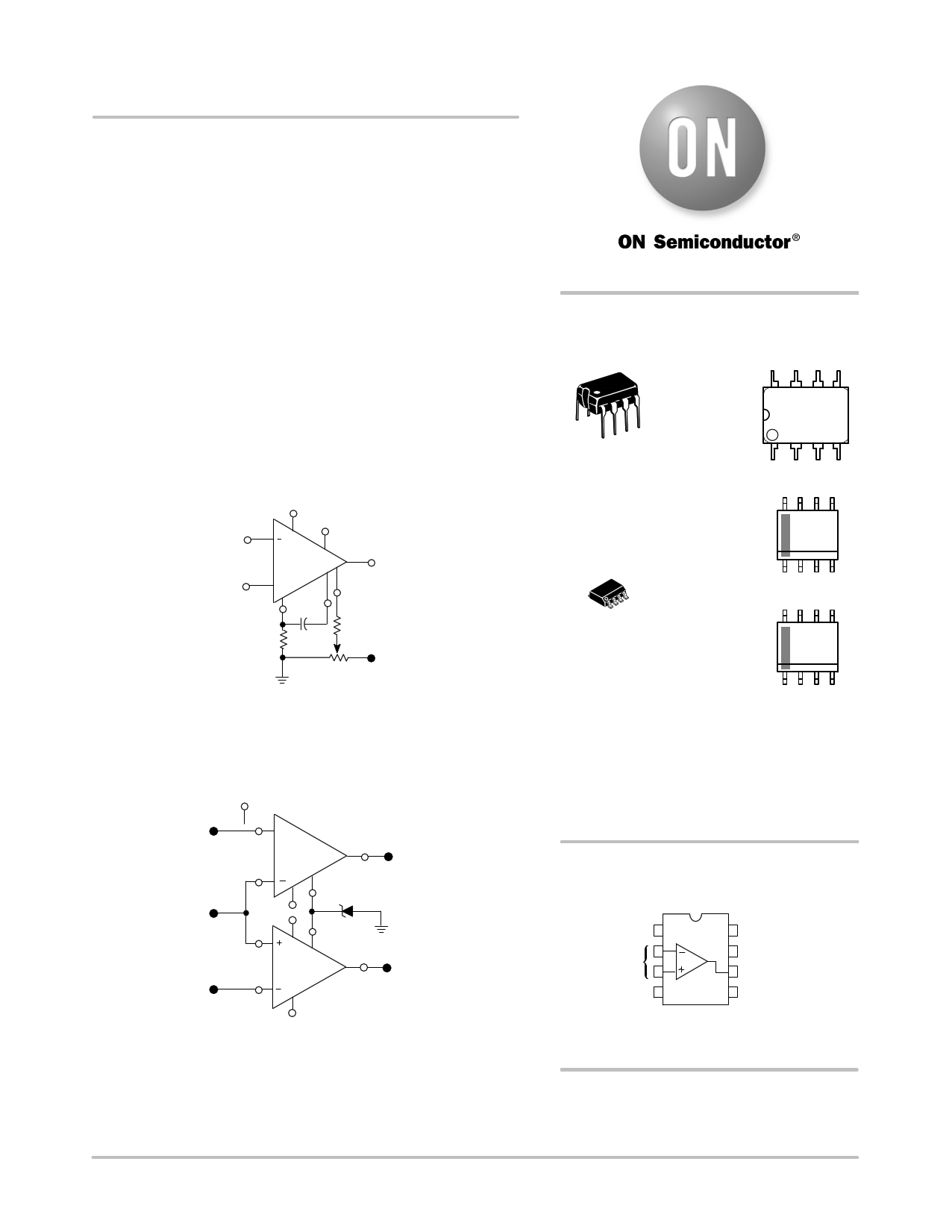
Inverting
Input
VEE
VCC
Non-
Inverting
Input +
Freq
Balance Compen
10 MW 30 pF
Output
Balance
5.1 MW
20 k VEE
Figure 1. Standard Compensation
and Offset Balancing Circuit
VUT VCC
+
VI VEE
VCC
VO
MZ4622 or Equiv.
3.9 V
VLT VO
VO = 4.8 V for
VLT ≤ VI ≤ VUT
VEE VO = -0.4 V
VI < VLT or VI > VUT
(Pins Not Shown Are Not Connected)
Figure 2. Double−Ended Limit Detector
© Semiconductor Components Industries, LLC, 2011
December, 2011 − Rev. 11
1
8
1
http://onsemi.com
PDIP−8
N SUFFIX
CASE 626
MARKING
DIAGRAMS
8
LMx01AN
AWL
YYWWG
1
8
1
SOIC−8
D SUFFIX
CASE 751
8
LMx01
ALYWA
G
1
LM201AVDR2G
8
201AV
ALYW
G
1
x
A
WL, L
YY, Y
WW, W
G
G
= 2 or 3
= Assembly Location
= Wafer Lot
= Year
= Work Week
= Pb−Free Package
= Pb−Free Package
PIN CONNECTIONS
Balance 1
2
Inputs
3
VEE 4
8 Compensation
7 VCC
6 Output
5 Balance
(Top View)
ORDERING INFORMATION
See detailed ordering and shipping information in the package
dimensions section on page 2 of this data sheet.
Publication Order Number:
LM301A/D
1 page 
LM301A, LM201A, LM201AV
10
8.0 Single-Pole Compensation
6.0
4.0
2.0
Input
0 Output
-2.0
-4.0
-6.0
-8.0
-10
0 10 20 30 40 50 60 70 80 90
t, TIME (ms)
Figure 10. Voltage Follower Pulse Response
140
120
Feedforward
Compensation
100 225
80 180
60
Phase
135
40 90
20 Gain 45
0 00
-20
10 100 1.0 k 10 k 100 k 1.0 M 10 M 100 M
f, FREQUENCY (Hz)
Figure 11. Open Loop Frequency Response
18
Feedforward
16 Compensation
12
8.0
4.0
0
100 k
1.0 M
f, FREQUENCY (Hz)
10 M
Figure 12. Large Signal Frequency Response
R2
R1
7 VCC
2
-VI 6
R3 3
+VI
+
48
VO
1 VEE
Frequency
Compensation
Balance
C1
C1 ≥
R1 Cs
R1 +R2
Cs = 30 pF
Figure 14. Single−Pole Compensation
10
Feedforward
8.0 Compensation
6.0
4.0
2.0 Input
0
-2.0
-4.0
Output
-6.0
-8.0
-10
0 1.0 2.0 3.0 4.0 5.0 6.0 7.0 8.0 9.0
t, TIME (ms)
Figure 13. Inverter Pulse Response
C2
R1
VI
R3
R2
2 7 VCC
6
3
+
1
C1
4
VEE
Balance
VO
150 pF
1
C2 =
2πfoR2
fo = 3.0 MHz
Figure 15. Feedforward Compensation
http://onsemi.com
5
5 Page | ||
| Páginas | Total 7 Páginas | |
| PDF Descargar | [ Datasheet LM201A.PDF ] | |
Hoja de datos destacado
| Número de pieza | Descripción | Fabricantes |
| LM20123 | LM20123/LM20123Q 3A 1.5MHz PowerWise Synchronous Buck Regulator (Rev. E) | Texas Instruments |
| LM20123 | Synchronous Buck Regulator | National Semiconductor |
| LM20124 | LM20124/LM20124Q 4A 1MHz PowerWise Synchronous Buck Regulator (Rev. F) | Texas Instruments |
| LM20124 | Synchronous Buck Regulator | National Semiconductor |
| Número de pieza | Descripción | Fabricantes |
| SLA6805M | High Voltage 3 phase Motor Driver IC. |
Sanken |
| SDC1742 | 12- and 14-Bit Hybrid Synchro / Resolver-to-Digital Converters. |
Analog Devices |
|
DataSheet.es es una pagina web que funciona como un repositorio de manuales o hoja de datos de muchos de los productos más populares, |
| DataSheet.es | 2020 | Privacy Policy | Contacto | Buscar |