|
|
PDF 74LVXZ161284 Data sheet ( Hoja de datos )
| Número de pieza | 74LVXZ161284 | |
| Descripción | Low Voltage IEEE 161284 Translating Transceiver | |
| Fabricantes | Fairchild Semiconductor | |
| Logotipo | ||
Hay una vista previa y un enlace de descarga de 74LVXZ161284 (archivo pdf) en la parte inferior de esta página. Total 11 Páginas | ||
|
No Preview Available !
May 2002
Revised May 2002
74LVXZ161284
Low Voltage IEEE 161284 Translating Transceiver
with Power-Up Protection
General Description
The LVXZ161284 contains eight bidirectional data buffers
and eleven control/status buffers to implement a full
IEEE 1284 compliant interface. The device supports the
IEEE 1284 standard and is intended to be used in an
Extended Capabilities Port mode (ECP). The pinout allows
for easy connection from the Peripheral (A-side) to the
Host (cable side).
Outputs on the cable side can be configured to be either
open drain or high drive (± 14 mA) and are connected to a
separate power supply pin (VCC-Cable) that allows these
outputs to be driven by a higher supply voltage than
the A-side. The pull-up and pull-down series termination
resistance of these outputs on the cable side is optimized
to drive an external cable. In addition, the C inputs and the
B and Y outputs on the cable side contain internal pull-up
resistors connected to the VCC-Cable supply to provide
proper input termination and pull-ups for open drain output
mode.
Outputs on the Peripheral side are standard low-drive
CMOS outputs designed to interface with 3V logic. The DIR
input controls data flow on the A1–A8/B1–B8 transceiver
pins.
This device also has an added power-up protection feature
which forces the Y outputs (Y9 - Y13) to a high state after
power-on until one of the associated inputs (A9 - A13) goes
HIGH. When an associated input (A9 - A13) goes HIGH, all
Y outputs (Y9 - Y13) are activated.
Features
I Supports IEEE 1284 Level 1 and Level 2 signaling
standards for bidirectional parallel communications
between personal computers and printing peripherals
I Translation capability allows outputs on the cable side to
interface with 5V signals
I All inputs have hysteresis to provide noise margin
I B and Y output resistance optimized to drive external
cable
I B and Y outputs in high impedance mode during power
down
I C inputs and B, Y outputs on cable side have internal 1.4
kΩ pull-up resistors
I Flow-through pin configuration allows easy interface
between the “Peripheral and Host”
I Replaces the function of two (2) 74ACT1284 devices
I Power-up protection prevents errors when the printer is
powered on but no valid signal is at the input pins
(A9 - A13).
Ordering Code
Order Number
74LVXZ161284MEA
74LVXZ161284MEX
74LVXZ161284MTD
74LVXZ161284MTX
Package
Number
MS48A
MS48A
MTD48
MTD48
Package Description
48-Lead Small Shrink Outline Package (SSOP), JEDEC MO-118, 0.300" Wide
[RAIL]
48-Lead Small Shrink Outline Package (SSOP), JEDEC MO-118, 0.300" Wide
[TAPE and REEL]
48-Lead Thin Shrink Small Outline Package (TSSOP), JEDEC MO-153, 6.1mm Wide
[RAIL]
48-Lead Thin Shrink Small Outline Package (TSSOP), JEDEC MO-153, 6.1mm Wide
[TAPE and REEL]
© 2002 Fairchild Semiconductor Corporation DS500729
www.fairchildsemi.com
1 page 
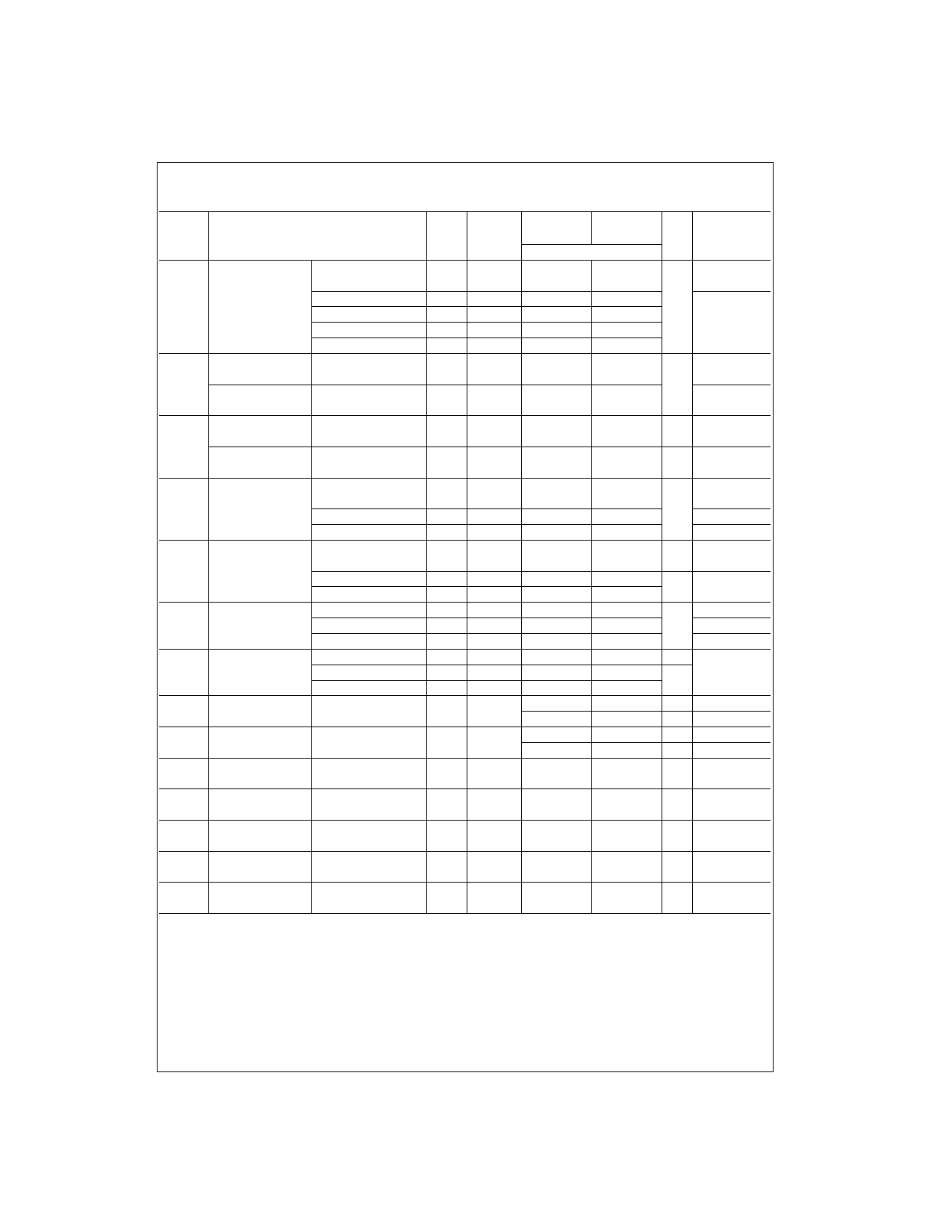
DC Electrical Characteristics (Continued)
Symbol
Parameter
VCC
(V)
VCC—Cable
(V)
TA = 0°C
TA = −40°C
to +70°C
to +85°C
Guaranteed Limits
Units
Conditions
VOL Maximum LOW
Level Output
An, HLH
Voltage
Bn, Yn
Bn, Yn
PLH
PLH
RD
Maximum Output
B1 - B8, Y9 -Y13
Impedance
Minimum Output
Impedance
B1 - B8, Y9 - Y13
3.0 3.0
3.0 3.0
3.0 3.0
3.0 4.5
3.0 3.0
3.0 4.5
3.3 3.3
3.3 5.0
3.3 3.3
3.3 5.0
0.2
0.4
0.8
0.77
0.85
0.8
60
55
30
35
0.2
0.4
0.8
0.77
0.95
0.9
60
55
30
35
IOL = 50 µA
IOL = 4 mA
V IOL = 14 mA
IOL = 14 mA
IOL = 84 mA
IOL = 84 mA
(Note 5)(Note 7)
Ω
(Note 5)(Note 7)
RP
IIH
IIL
IOZH
IOZL
IOZPU
IOZPD
IOFF
Maximum Pull-Up
B1 - B8, Y9 - Y13,
Resistance
C14 - C17
Minimum Pull-Up
B1 -B8, Y9 - Y13
Resistance
C14 - C17
Maximum Input
A9 - A13, PLHIN,
Current in
HD, DIR, HLHIN
HIGH State
C14 - C17
C14 -C17
Maximum Input
A9 - A13, PLHIN,
Current in
HD, DIR, HLHIN
LOW State
C14 - C17
C14 - C17
Maximum Output
A1 - A8
Disable Current
B1 - B8
(HIGH)
B1 - B8
Maximum
A1 - A8
Output Disable
B1 - B8
Current (LOW)
B1 - B8
Maximum Power-Up Y9 - Y13
Disable Current
B1 - B8
Maximum Power-Down Y9 - Y13
Disable Current
B1 - B8
Power Down
B1 - B8, Y9 - Y13,
Output Leakage
PLH
3.3 3.3
3.3 5.0
3.3 3.3
3.3 5.0
3.6 3.6
3.6 3.6
3.6 5.5
3.6 3.6
3.6
3.6
3.6
3.6
3.6
3.6
3.6
3.6
0 to 1.5
(Note 8)
0 to 1.5
(Note 8)
3.6
5.5
3.6
3.6
5.5
3.6
3.6
5.5
0 to 1.5
(Note 8)
0 to 1.5
(Note 8)
0.0 0.0
1650
1650
1150
1150
1.0
50.0
100
−1.0
−3.5
−5.0
20
50
100
−20
−3.5
−5.0
350
−5
350
−5
100
1650
1650
1150
1150
1.0
50.0
100
−1.0
−3.5
−5.0
20
50
100
−20
−3.5
−5.0
350
−5
350
−5
100
Ω
Ω
VI = 3.6V
µA
VI = 3.6V
VI = 5.5V
µA VI = 0.0V
mA VI = 0.0V
VO = 3.6V
µA VO = 3.6V
VO = 5.5V
µA
mA VO = 0.0V
µA VO = 5.5V
mA VO = 0.0V
µA VO = 5.5V
mA VO = 0.0V
µA VO = 5.5V
IOFF
Power Down
Input Leakage
C14–C17, HLHIN
0.0 0.0
100
100 µA VI = 5.5V
IOFF—ICC Power Down
Leakage to VCC
IOFF—ICC2 Power Down Leakage
to VCC—Cable
ICC Maximum Supply
Current
0.0 0.0
0.0 0.0
3.6 3.6
3.6 5.5
250
250
45
70
Note 5: Output impedance is measured with the output active LOW and active HIGH (HD = HIGH).
250 µA (Note 6)
250 µA (Note 6)
45 mA VI = VCC or GND
70 mA VI = VCC or GND
Note 6: Power-down leakage to VCC or VCC—Cable is tested by simultaneously forcing all pins on the cable-side (B1–B8, Y9–Y13, PLH, C14–C17 and HLHIN)
to 5.5V and measuring the resulting ICC or ICC—Cable.
Note 7: This parameter is guaranteed but not tested, characterized only.
Note 8: Connect all VCC pins and VCC-Cable pins when forcing voltage applied, DIR = HD = 0V.
5 www.fairchildsemi.com
5 Page 
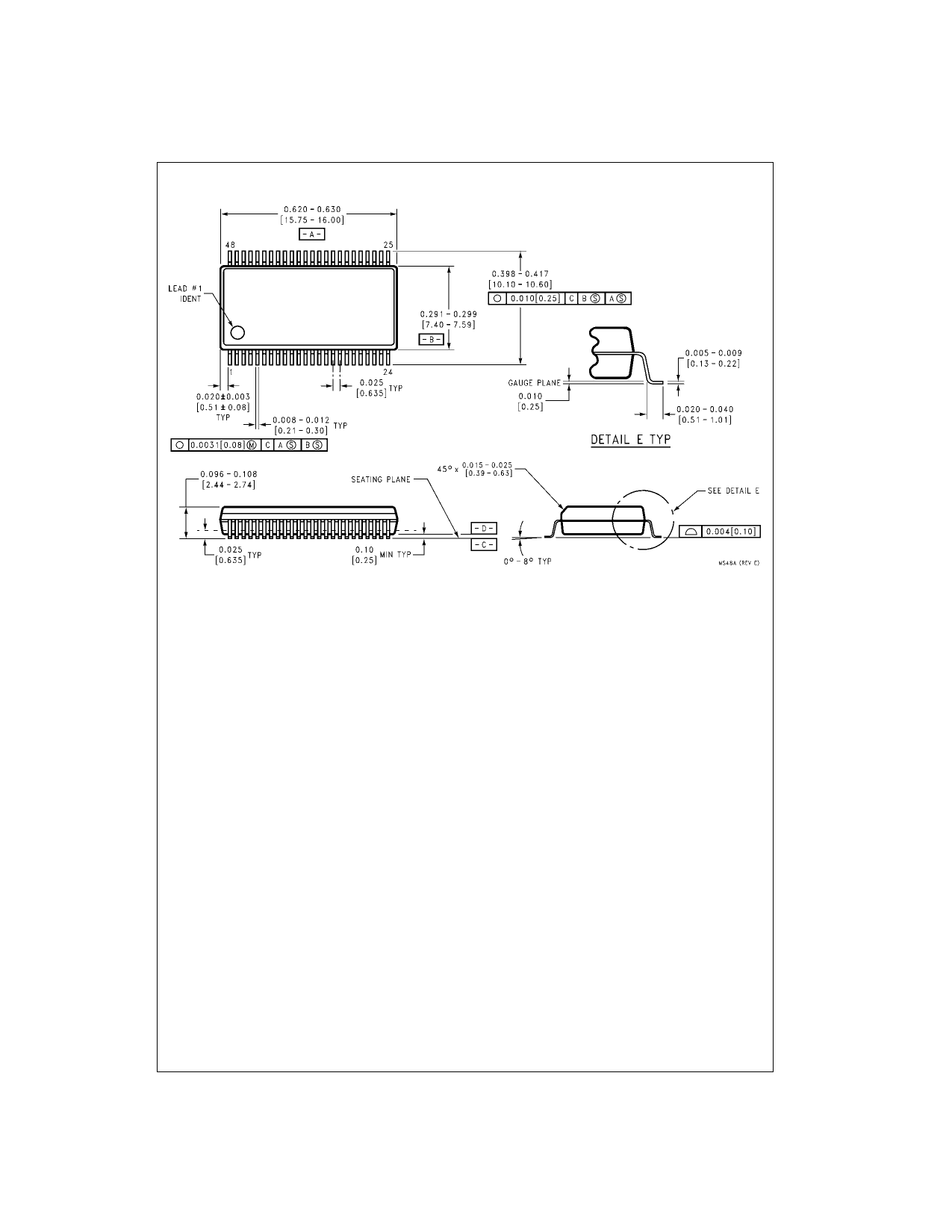
Physical Dimensions inches (millimeters) unless otherwise noted
48-Lead Small Shrink Outline Package (SSOP), JEDEC MO-118, 0.300" Wide
Package Number MS48A
11 www.fairchildsemi.com
11 Page | ||
| Páginas | Total 11 Páginas | |
| PDF Descargar | [ Datasheet 74LVXZ161284.PDF ] | |
Hoja de datos destacado
| Número de pieza | Descripción | Fabricantes |
| 74LVXZ161284 | Low Voltage IEEE 161284 Translating Transceiver | Fairchild Semiconductor |
| Número de pieza | Descripción | Fabricantes |
| SLA6805M | High Voltage 3 phase Motor Driver IC. |
Sanken |
| SDC1742 | 12- and 14-Bit Hybrid Synchro / Resolver-to-Digital Converters. |
Analog Devices |
|
DataSheet.es es una pagina web que funciona como un repositorio de manuales o hoja de datos de muchos de los productos más populares, |
| DataSheet.es | 2020 | Privacy Policy | Contacto | Buscar |
